Sunday, October 25, 2015

Short Circuit - Part 2

I finally managed to stack up the robot i have been building. The completed assembly is shown in the photo below. The robot can be remotely controlled as far as the NRF24L01+ with PA can allow and can transmit video over a WiFi connection. Video transmission is therefore limited to the range of the WiFi signal.


This article is a follow-up to a previous one that you can find here. Read this First !!!

[1] The foundation of the robot is a Zumo robot shield from Polulu containing the power source - batteries, gyro etc. 


[2] The zumo motors are controlled by an arduino clone called Entuino from Entesla. I had this board modified such that the header pins stick out of the bottom of the board so that i could mount custom shields on top of the main board. The DC jack had to be de-soldered too. This processor runs a state machine that controls the motors based on commands it gets from [3]


[3] I designed a custom board to mount the Teensy 3.1 ARM Cortex M3 module from PJRC. This board was stacked on top of the Entuino. The purpose of this board is to communicate with the NRF24L01+ 2.4 GHz radio transceiver and send the commands down below to the Ent. This board will also process the data obtained from the gyroscopes on the zumo shield. The reason behind using the Teensy was to offload the communication and computing from the ATMega, as it has more features and memory and use the Ent only for motor control.

As seen below the plastic mount is fastened to [3] using M3 bolts and slots cuts in the board & rests on header pins. I could have removed the pins but that would render the board useless for any other future projects. Hence, bob's your uncle....go figure...


[4] The last board on the stack is the RaspberryPi. It's sole purpose is to provide camera data over Wifi. On power up a remote login is made over wifi to access the RPi terminal, from the terminal a VNC server is started. Using a windows VNC client like TightVNC the remote VNC session is accessed providing the RPi desktop. Once on the desktop the camera can be accessed using OpenCV. The motion of the robot can now be controlled using another arduino with a NRF24L01+ connected to the PC serial port and you can view where the robot is going using the WiFi VNC session. There is a minor N/W delay in viewing the video over VNC.

I had to design a custom 3D printed part to mount the RPi board and it's camera. The part was printed using my FabX 2.0 printer. Some slots had to be cut out in board [3] using a dremel to mount the M3 bolts to fasten the 3D printed mount. The part went through several iterations to get the dimensions, thickness and placement right.


Design Iteration 1: The one on the left was too thin and bent under the pressure of the bolts given that the bolts did not align properly to the RPi holes due to inherent 3D printer drifts. The camera mount was totally miscalculated.

Design Iteration 2: The one in the center turned out fine but the camera mount slot turned out too wide because of a small dimension miscalculation in SolidWorks. Additionally the through-hole components of the RPi were causing misalignment when the fastening bolts were tightened. I removed some material from the center of the base plate and filleted the corners to speed up printing and use less filament.

Design Iteration 3: The one on the right turned out perfect but the camera mount had the same problem of not going into the slot enough. Though it was a tight fit, the camera was resting on the components on the bottom layer of the camera board which was not good. I would rather prefer to rest it on the camera edge cable connector.

Design Iteration 4: The one at the bottom and the last one finally turned out to be just right. The RPi mounting holes were extruded above the base plate to give a flat mount with a support at the end of the base plate, this prevented any through hole components from touching the plastic.. The camera mount was extended to the bottom and some material was removed such that it went right through the slot and came to rest on the edge connector. Instead of using holes i replaced them with rounded slots so that the bolts can be aligned properly with the mounting holes on the RPi to correct for drifts in intended design by the printer.


The above design can be found on my Thingiverse along-with other stuff.

A lot of mods have been planned to keep the stacking of boards to a minimum and have everything controlled using the RaspberryPi in the near future.

Thursday, July 2, 2015

Dual-OS Co-existence on Single Core

Coming Soon
uC-OS III running "with" FreeRTOS on a single core Cortex-A8


Due to uC-OS III licensing issues i cannot post details about this implementation.


Fin

Thursday, June 18, 2015

FreeRTOS on Cortex-A8 FVP ARM DS-5

Here is an implementation of the FreeRTOS ARM Cortex-A port on the DS-5 Cortex-A8 Fixed Virtual Platform. I was planning to do this since a long time (as my beagleboard went up in magic smoke and i did not have any platform to experiment on) and now that it is finally done, you can evaluate FreeRTOS on a Cortex-A series processor without the need to purchase additional hardware. Students and professionals can also explore RTOS concepts / design methodologies or even tweak the OS, try real nasty things. This implementation is now available at my GitHub.

I am unaware of existing FVP implementations. I could not find any by doing a Google search. Hence, if you are aware of any such implementation please link in the comments below. Compiled and tested in ARM DS-5 Ultimate Edition (Evaluation) Version: 5.21.0 Build number: 5210017

Most of the information can be figured out by going through the code, by doing a diff of the source file with the original, however some brief implementation details are mentioned below.

Keep this document handy as it contains the memory map of the FVP. Also note that this is a simulation and will not be "real-time". This project is only to understand the inner workings of FreeRTOS or any RTOS in general. To run it on real hardware you will still need the board specific settings. For that refer to my earlier post on FreeRTOS with the BeagleBoard. Turn on Rate-Limit in the CLCD screen for stable response if required.

Import this project into DS-5. Compile and create a Debug Configuration for the Cortex-A8 FVP Bare-Metal debug.

The system is configured for a maximum 32 interrupts. The FVP has 64 interrupt sources out of which the first 16 are SGIs. More information on interrupt priority assignments on Cortex-A series specific to this OS can be found here.

I am using the SP804 Timer Module 0 to generate the tick interval. The timer is configured as a 32-bit counter, periodic timer. timer_init.s has a minimal assembly implementation.

The port for the Cortex-A series can be found in the FreeRTOS portable directory - \FreeRTOSV8.2.1\FreeRTOS\Source\portable\RVDS\ARM_CA9.

configCPU_CLOCK_HZ and configPERIPHERAL_CLOCK_HZ would really not matter in the simulation. The tick timer has been configured with a value of 0x3e8. The FreeRTOSConfig.h file has been used by modifying the one in Renesas demo project.

As this will be running on a Cortex-A8 FVP, the Cortex-A8 startup file can be found in the bare-metal examples directory in the DS-5 installation. This file has been modified for the current implementation by adding stack initialization, enabling GIC etc.

Additional changes in port.c for handling the tick and setting API for clearing the timer interrupt.

main.c implements 3 tasks for demonstration:
RollingLEDSTask - This task nudges the LEDs in the CLCD window one at a time, prints the number of times it's called and goes to sleep for 1 tick.

PrintHelloTask - Prints hello world to the console and the number of times it is called and goes to sleep for 5 ticks.

PrintKeyboardTask - I was looking for a method to externally trigger events in the DS-5 debugger. Unfortunately the GPIO controller in the FVP lacks this capability. Therefore the only method was to use the PL050 implementation in the FVP to trigger events using the keyboard connected to the computer :P

PL050.c therefore contains a minimal implementation of the driver for this FVP peripheral. the PrintKeyboardTask blocks on a semaphore on start up. If a key is pressed on the keyboard while the CLCD window is active, the PL050 generates 3 interrupts. The 3 bytes sent in sequence are [scancode], [0xF0], [scancode] Leave a comment below if you know why 3 bytes. The first byte is indeed the scan-code but i have no idea what the second byte is. Ideally it should be the shift key status. On the third interrupt the semaphore is released from the IRQ handler of the peripheral which activates the task to print out to the console. To get the ascii value of the key, you might have to convert the scancode to the corresponding ascii value. For character - a, i was getting scan code of 0x1C which might differ based on your locale / keyboard type.

P.S: Most files are in assembly and not in C e.g the timer and GIC APIs, the reason being - i already had these ready from earlier projects, hence used the same. You can use your own implementation in C if you require. 

To enable FreeRTOS awareness in DS-5 please enable the flags mentioned in this article on ARM Infocenter.

If you have any questions leave a comment below. Few screenshots of my tool settings are shown below.


Available on FreeRTOS interactive site

http://interactive.freertos.org/entries/83853195-FreeRTOS-on-Cortex-A-FVP-ARM-DS-5


Saturday, April 4, 2015

FreeRTOS on Xilinx Zynq Zybo [Single Core]

This post will guide you in getting FreeRTOS up and running on the Zybo Zynq 7000 development board from Digilent. The post will focus on running FreeRTOS on a single core. After a few eons i shall be putting up another post on running FreeRTOS, each on one core. The entire project has been uploaded to Git and the link is somewhere down below.

What we are going to do ?
1. Create a custom AXI4 Lite peripheral whose output port will be connected to the four LEDs on the Zybo.

2. Get FreeRTOS to run on the ZYBO.

3. Create a task in FreeRTOS to write data to the AXI peripheral and display it on the LEDs.

Pre-requisites:
1. The Zybo board.
2. Latest FreeRTOS source code.
3. Vivado 2014.x and Xilinx SDK 2014.x.
4. Knowledge of using the Xilinx tools.

Steps:
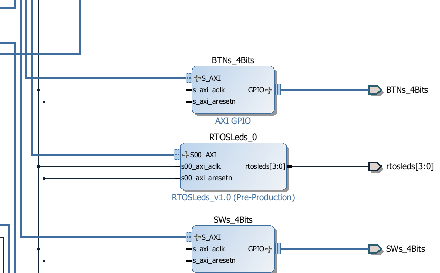
1. The first step is to build and setup  the hardware in Vivado. To keep this post short i would recommend you to click here and follow the Embedded Linux Tutorial by Digilent. You only need to refer this post on how to create a AXI Lite peripheral, section 1 - Hardware Customization and generate the Bitstream. It's upto you to work in VHDL or Verilog. I know VHDL therefore i had to delete the system_wrapper, change the Project Settings and regenerate the system_wrapper and other code in VHDL. Here is my custom AXI 4 LITE peripheral - RTOSLeds_0. Make sure that you assign address to your peripheral in the Address Editor before generating the bitstream.


2. Once you've finished generating the bitstream export it and Launch the SDK.

3. Within the SDK create a new application project, preferably a blank one or the HelloWorld project.
This should generate the BSP and the hello world project files. Now since we will not be using the helloworld.c file, we can delete it. Additionally remove the helloworld reference from the Makefile (that's if you created a helloworld project instead of a empty one).

4. On the FreeRTOS website there is a page that describes porting it to the Zynq processor. You will find the same project at this path in your FreeRTOS directory - \FreeRTOSV8.2.1\FreeRTOS\Demo\CORTEX_A9_Zynq_ZC702. The platform and BSP in that folder are not for the Zybo board therefore we do not need to refer those folders at all since we have created our own hardware and bsp in the steps above.

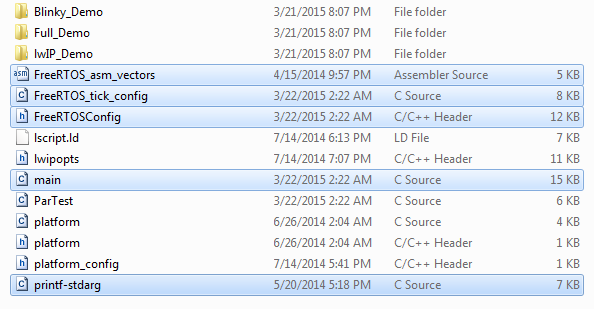
5. The  RTOSDemo folder which is our folder of interest contains the necessary files that need to be imported to our project workspace. Not all files, just a few that are highlighted below. The platform related files will already be present in the project.

Copy the above highlighted files to the src folder of the sdk project.

6. Navigate to the - \FreeRTOSV8.2.1\FreeRTOS\Source\portable\GCC\ARM_CA9 folder and copy port.c, portASM.S and portmacro.h to the xilinx sdk src folder.

7. Navigate to the - \FreeRTOSV8.2.1\FreeRTOS\Source folder and copy all the six  C files to the project.

8. Copy the FreeRTOS headers from the include directory at the same path [7] into the xilinx sdk.

9. Copy  heap_4.c from the \FreeRTOSV8.2.1\FreeRTOS\Source\portable\MemMang directory into the project directory.

10. Your Xilinx SDK project src folder should now contains all the files as shown below.


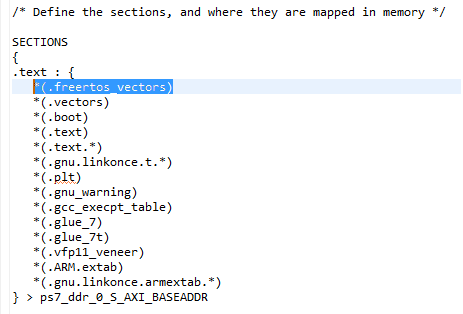
11. The next important thing that needs to be changed is the linker script file - lscript.ld. There is only one new line to be added here as highlighted below.


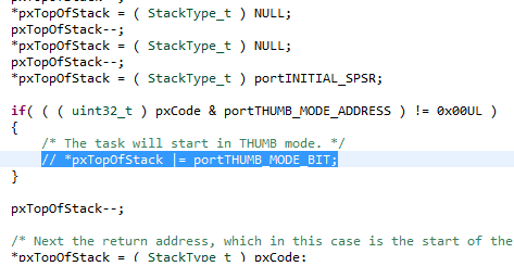
12. I do not want my code to run in thumb mode. Therefore i commented out the line shown below in the function pxPortInitialiseStack present in file port.c. In FreeRTOSConfig.h change the configCPU_CLOCK_HZ macro to 50Mhz.


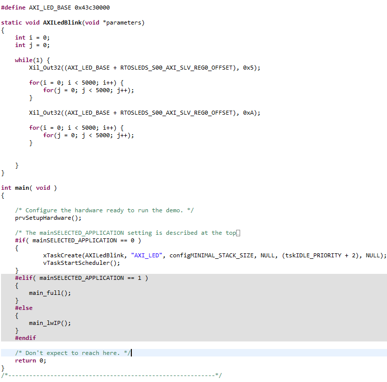
13. To test it all out i created a simple task that would send the data 0x5, 0xA alternately after a fixed delay to the AXI peripheral thereby displaying the pattern on the zybo leds.


14. The last step is the comment out the call to vParTestInitialise() from the prvSetupHardware function as it is not related to the Zybo board.

15. Well, after the above steps, if everything compiles correctly without errors, program the FPGA and the ELF using the Xilinx Tools menu and start the debug session. Make sure you have the Zybo powered up from the wall adapter and the JP5 header set to JTAG. In my case the USB power did not work as the level shifters were not enabled when i used it.

FreeRTOS on the Digilent Zybo....done...

The entire project on GitHub: 

My other FreeRTOS adventures:


Thursday, February 26, 2015

Samsung S-Pen Internals

The S Pen, introduced with the Galaxy Note, is faster and more accurate than conventional stylus pens. It is an input tool that provides a similar feel to an actual pen by detecting the pressure applied on the screen with great accuracy (wait, what....) [Source]

I was lucky to get my hands on a spare S Pen which turned out to be not so lucky for the pen. This post will explore the S Pen internals, crack it open, hook it up to a scope etc.

Cracking the Pen
The S Pen is a very robust design and it's internal circuitry cannot be easily accessed. You will have to use a saw or a dremel to carefully cut it open. I used a dremel to mercilessly slaughter the S Pen. The best position to start sawing would be at a distance of about 80 mm from the tip of the pen. Then slowly working your way up towards the tip till you reach a printed circuit board capped with a small plastic holder as shown in the images below. The pcb assembly slides outwards away from the tip. You will have to remove the plastic button in order to remove the pcb effortlessly.


The S Pen disassembled. Top PCB and bottom side

A close up of the components on the pcb is shown below. Starting from the tip we have the coil assembly consisting of a 0.22 mm dia (approx.) wire wound on a soft iron core which is not cylindrical. The tip is connected to a spring at the base of the assembly which appears to be some kind of switch or a variable capacitor. I believe this assembly consisting of the spring deals with the pressure sensing, either by bringing the coil close to the display surface by compressing the spring or by using the contacts at the base of the assembly as a variable parallel plate capacitor. We then have the push button that is usually used for the air command interface followed by two sensitivity adjustment potentiometers and a bunch of capacitors connected in parallel to the coil thereby forming an LC resonant circuit. The little solder blobs below each capacitor are jumper connections. Therefore as shown below, from left to right the first capacitor and the last capacitor are not connected in parallel with the coil. If you are wondering where is the circuit diagram.....it's coming soon....

Close up of the PCB


Operating Principle

Samsung partnered with Wacom to develop the S Pen. The pen works on the principle of Electro-Magnetic Resonance (EMR). Devices utilizing EMR Technology do not require any cable or built-in battery-based power supply at all. This is because the cellphone incorporates a sensor board beneath the OLED display that detects the pen's movement. Weak energy is induced in the pen's resonant circuit by a magnetic field generated by the sensor board surface. The pen's resonant circuit then makes use of this energy to return a magnetic signal to the sensor board surface. By repeating this movement, the board detects information on the pen's coordinate position and angle, as well as on its general operating condition including speed and writing pressure, etc. A sensor unit is equipped at the side of the sensor board to switch the magnetic field on and off and to receive signals at high speed and detect various kinds of information. In principle, all Wacom's tablet devices are composed of this kind of sensor unit and electronic pen. In addition, the sensor unit itself consists of a sensor board and a control board.

The sensor board is an array of tiny loop antennas arranged in overlapping X and Y directions. The control board switches a high frequency signal into each of the loop antenna coils. This causes them to generate a magnetic field. When the pen passes through this magnetic field, it picks up and stores energy in it's resonant circuit. The control board then instantaneously switches to the receiver and roughly determines the pen's location by scanning all the loop coils. After that, the control board scans multiple loop coils in the vicinity of the pen, and uses the information to calculate the pen's coordinate value precisely. The control board has its own custom DSP circuit performing all the high speed calculations.

For example, let's take the Samsung Galaxy Note 2. The internal view of the Note is shown below. Notice the golden panel. That is the sensor board - the digitizer that interacts with the S Pen [Source]


Hooking it Up

In order to see what is going on inside the S Pen circuitry i connected some wires to the coil pads on the pcb and hooked it up to my oscilloscope. The device operates at a certain carrier frequency as shown below. The signal is power optimized and the data transaction is in some frames that i observed in a repetitive pattern. The same pattern seems to shape-shift when the S Pen is oriented to the display at different angles.Refer to the text below each image for more information. The scope waveform was very jumpy and the values mentioned are close approximate readings off the scope.


Each frame is approximately 15 ms. The above pattern repeats over and over.


Here is the same 15 ms frame but it appears different because the pen was oriented at an angle of around 30 degrees (back end towards the home key) with the surface of the display


Here is the same 15 ms frame but now oriented at an angle of around 120 degrees (back end away from home key) with the surface of the display


Let's turn that time base down


The carrier frequency appears to be approximately 560 KHz


The FFT of the signal gives a strong peak around 560 KHz


Wonder what happens when you push the small button on the S Pen ? The 560 KHz peak shifts to 530 KHz. I guess this frequency shift gets detected as a button press by the sensor board. Pressing the switch must be connecting additional capacitance in the LC parallel circuit thereby changing its resonant frequency. Barely noticeable in the image, but if you click on the image and switch to the image viewer you can alternate between image numbers 8 and 9 using the arrow keys to observe the shift.


This is the frequency response of the LC parallel resonant circuit of the S Pen which was obtained by sweeping a sine wave from 100 KHz to 1 MHz at the coil terminals, with the coil connected to the PCB. The dip is at around 565 KHz.

In a nutshell, the phone containing the "digitizer" or sensor board generates a magnetic field that induces a current in the coil that is connected to the parallel LC tank circuit, the sensor board then switches into receiving mode, letting the resonant energy drain through the S Pen coil thereby detecting it's position, pressure and angle. 

Let's  go back to the first paragraph of this post referenced from another post stating "detecting the pressure applied on the screen". Well, nope. The statement is framed incorrectly leading anyone to believe there are pressure sensors on the screen for the S Pen. But as we found out, it is not so...

The S Pen therefore accomplishes a lot with simple circuitry and basic principles of electromagnetism. Michael Faraday will be proud :P

These observations are based on the S Pen i own using the Digilent Analog Discovery. If you perform the same set of experiments and get to know something new and weird or decode the frame structure if any, comment below. Found a mistake in the text ? comment below...

For information on LC resonant circuits check out the video below:


Sunday, February 1, 2015

Short Circuit - Part 1

I've  got my hands on the Zumo 1.2 robot and it's time to do some crazy stuff with it. Last month i finished designing a customized baseboard for the Teensy 3.1 Cortex-M4 board by PJRC. This baseboard was tailored specifically for the Zumo. More details on the Zumo 1.2 can be found here. The zumo is designed such that it acts as a shield for the arduino uno board. However if you mount the standard original arduino on the zumo, you cannot mount other shelds. Some pins are specific to the Zumo which you can check on the Zumo wiki. Some of my friends who are founders of Entesla managed to give me one of their arduino clones - the Entuino with all the headers removed. I soldered the new headers as per my convienience, removed the DC jack and reset switch and it looks like this.


When mounted on the Zumo the board looks like this. Now i can mount an infinite number shields on top of this board (conditions apply....even mathematically :P)


Notice that few of the pins have been cut off such that they do not interfere with the shield on top. These are primarily the controls for the zumo motors that were mapped to the same pins used by SPI. The power pins too were not made available to shields above the entuino. The Teensy board has its own voltage regulators for 5V and 3.3 V and hence sources from the Vin supply from the Zumo shield which is 7.5 V


I will be using the arduino for the sole purpose of controlling the motors. All the sensors' data computation will be taken care by the Teensy over the I2C bus. The teensy and entuino communicate with each other via the hardware UARTs, (0, 1) on the entuino and (0,1) Serial1 on the Teensy. The Teensy also has a NRF24L01+ interfaced over the SPI bus for remotely controlling the bot and for data telemetry. The Teensy base board also has support for the ESP8266 wifi (not connected) and a 40 pin header to connect the Raspberry Pi. The Teesny baseboard and the RPi communicate over the UART. The whole block diagram of the entire system is shown below. Currently the ESP8266 and RPi are not connected to the teensy baseboard. Initially i had planned to use the SoftwareSerial library on the teensy for comms between teensy and entuino, but that backfired as the SoftSerial library is defunct. Therefore, i patched the ESP uart to the hardware uart of the entuino (the white wires in pics below).


The fully assembled robot.


The two boards


Now i have to take utmost care to solder the 40 pin header whose component side is behind the board. R.I.P ESP8266. #facepalm, softwareserial #fail.


The Eagle schematic. Not perfect i must say, jeez, look at some vias and those clearances... :P


Fully Powered Up


More adventures with this in Short Circuit - Part 2.