The ARM FastModels series of posts will be focusing on building a simple SoC from scratch, bringing up FreeRTOS on the SoC, creating a custom IP using the native language LISA and porting of the SMSC91C111 Ethernet controller driver on the virtual platform. The links to each of the below topics will be enabled once the post is ready for hosting.
- 1. The SoC hardware architecture.
- 2. Bringing up Free RTOS on the SoC.
- 3. Adding a custom peripheral IP.
- 4. Porting the Network Controller driver.
I have been playing around with FastModels for quiet some time and it is a fascinating tool to design and build your own SoC Virtual Prototype from scratch and learn the process of interfacing various IPs to the SoC. More information on FastModels can be found
here. It is available for a 30 day trial for a processor of your choice. I chose the Cortex-A5 MPCore processor and therefore the SoC will be designed around it. Using the tool-chain is pretty basic and can be almost easily followed through using the available user guides. Remember i said 'almost'. Most advanced features and IPs are not well documented or are proprietary and it could give you a concussion if you try to interface them.
If you are running on Windows then you need a full version of Visual Studio 2013 to compile the simulation ISIM executable. On Linux you can use the freely available gcc 4.8 compiler. I am using FastModels 10 on a Windows machine with a VS2013 60-day trial.
For my SoC code-named RAVEN i decided to go for a simple hardware architecture that consisted of a Cortex A5 Quad Core processor clocked at 500 MHz, PL011 UART IP, 1GB of RAM, SMSC91C111 Ethernet controller. This being a simulation, not all core features are available. To check out the features that are available for the Cortex A5MPCore model view the DUI0834H Fast Models reference manual section
3.2.15.
The Cortex-A5 model can provide full functional simulation of the ARM v7 architecture and comes bundled with the SCU, GIC, Private timer and WDT per core, one Global Timer and an Advanced Coherency Port. You can refer the A5 MPCore reference manual
here.
The FastModels design environment is a code based and block design based IDE akin to a Visual Programming IDE where you can drag and drop various IPs and connect them. If you have used tools like Xilinx Vivado or Multisim bob's your uncle. The scripting language is called LISA and is similar to C++.
The final SoC is shown above. Starting from the left -
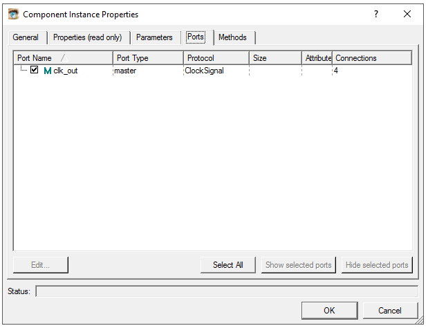
XTAL: The Master Clock IP. a clock signal of 1 Hz is available at the clk_out port of this IP. The clk_out master port follows the ClockSignal protocol and can only be connected to another IP that has a port e.g. clk_in declared as a slave port with ClockSignal protocol. A list of available protocols is in the reference manual. To view the IP properties, right click the IP block and select Object Properties which brings up the following dialog box.
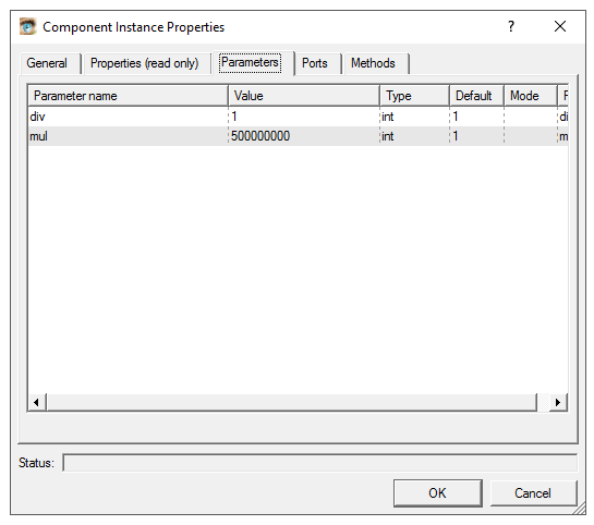
CORE_CLK: This is a Clock Divider IP. This IP can either multiply or divide the clock frequency that is input at its
clk_in terminal. The new clock signal comes out of the
clk_out signal. This IP has been used to provide the clock frequency for the Cortex-A5. As shown below the
mul parameter of this IP is 500000000. Since the input to the divider is 1 Hz it is multiplied by 500000000 to give a frequency of 500 MHz.This output is connected to the clk_in port of the processor.
PERIPHERAL_CLK: This is again a Clock Divider with the mul parameter set to 166666666 i.e. 166.66 MHz. FastModels provide a functionally accurate simulation of the system and not a timing accurate hence these clock values seldom do not influence functional verification. However, according to the datasheet the peripheral clock must be an integral multiple [N] of the core clock period with the multiple being greater than or equal to 2. Given a 500 MHz clock with 2ns period selecting N = 3 gives a 3:1 ratio and the peripheral clock period as 6ns hence 166.66 MHz.
UART_CLK and ETHERNET_CLK: The clock dividers for the UART and ETHERNET IPs clocked at 15MHz and 25 MHz respectively.
BUSDECODER0: The bus decoder IP is responsible of routing the bus transactions to the respective slave devices on the bus.The transactions on the PVBus are similar to AXI transactions. As shown, this IP is connected to the pvbus_m port of the processor which is one of the MASTER AXI ports. Each of the slave interfaces on the pvbus_m_range master port must be configured with a base address and size of the slave peripheral which must be 4KB aligned. This forms the memory map for the peripherals as shown below.
Now then, i figured that it is just impossible to type everything in here. The best thing would be to demonstrate the entire design process. Here is the video of the SoC design in action !!
After the build is successful a isim executable will be created in a release/debug directory inside the project folder. This executable needs to be imported into DS-5 to run the software and for simulations.


