Showing posts with label rishi franklin. Show all posts

Saturday, April 4, 2015

FreeRTOS on Xilinx Zynq Zybo [Single Core]

This post will guide you in getting FreeRTOS up and running on the Zybo Zynq 7000 development board from Digilent. The post will focus on running FreeRTOS on a single core. After a few eons i shall be putting up another post on running FreeRTOS, each on one core. The entire project has been uploaded to Git and the link is somewhere down below.

What we are going to do ?
1. Create a custom AXI4 Lite peripheral whose output port will be connected to the four LEDs on the Zybo.

2. Get FreeRTOS to run on the ZYBO.

3. Create a task in FreeRTOS to write data to the AXI peripheral and display it on the LEDs.

Pre-requisites:
1. The Zybo board.
2. Latest FreeRTOS source code.
3. Vivado 2014.x and Xilinx SDK 2014.x.
4. Knowledge of using the Xilinx tools.

Steps:
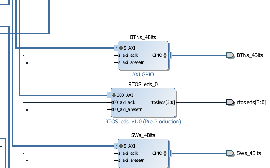
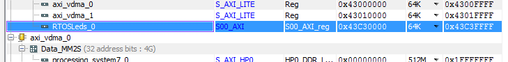
1. The first step is to build and setup  the hardware in Vivado. To keep this post short i would recommend you to click here and follow the Embedded Linux Tutorial by Digilent. You only need to refer this post on how to create a AXI Lite peripheral, section 1 - Hardware Customization and generate the Bitstream. It's upto you to work in VHDL or Verilog. I know VHDL therefore i had to delete the system_wrapper, change the Project Settings and regenerate the system_wrapper and other code in VHDL. Here is my custom AXI 4 LITE peripheral - RTOSLeds_0. Make sure that you assign address to your peripheral in the Address Editor before generating the bitstream.


2. Once you've finished generating the bitstream export it and Launch the SDK.

3. Within the SDK create a new application project, preferably a blank one or the HelloWorld project.
This should generate the BSP and the hello world project files. Now since we will not be using the helloworld.c file, we can delete it. Additionally remove the helloworld reference from the Makefile (that's if you created a helloworld project instead of a empty one).

4. On the FreeRTOS website there is a page that describes porting it to the Zynq processor. You will find the same project at this path in your FreeRTOS directory - \FreeRTOSV8.2.1\FreeRTOS\Demo\CORTEX_A9_Zynq_ZC702. The platform and BSP in that folder are not for the Zybo board therefore we do not need to refer those folders at all since we have created our own hardware and bsp in the steps above.

5. The  RTOSDemo folder which is our folder of interest contains the necessary files that need to be imported to our project workspace. Not all files, just a few that are highlighted below. The platform related files will already be present in the project.

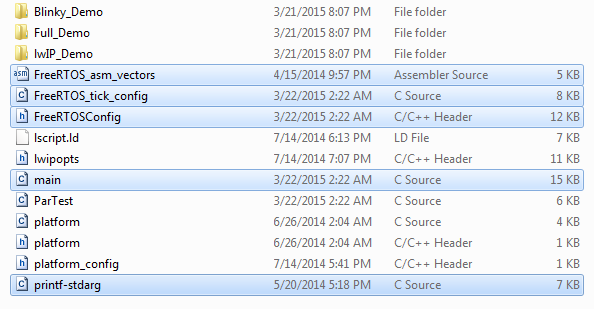
Copy the above highlighted files to the src folder of the sdk project.

6. Navigate to the - \FreeRTOSV8.2.1\FreeRTOS\Source\portable\GCC\ARM_CA9 folder and copy port.c, portASM.S and portmacro.h to the xilinx sdk src folder.

7. Navigate to the - \FreeRTOSV8.2.1\FreeRTOS\Source folder and copy all the six  C files to the project.

8. Copy the FreeRTOS headers from the include directory at the same path [7] into the xilinx sdk.

9. Copy  heap_4.c from the \FreeRTOSV8.2.1\FreeRTOS\Source\portable\MemMang directory into the project directory.

10. Your Xilinx SDK project src folder should now contains all the files as shown below.


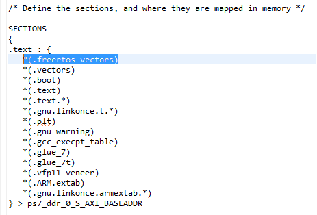
11. The next important thing that needs to be changed is the linker script file - lscript.ld. There is only one new line to be added here as highlighted below.


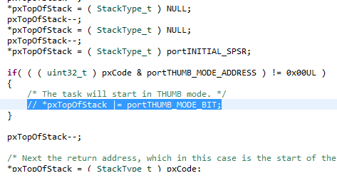
12. I do not want my code to run in thumb mode. Therefore i commented out the line shown below in the function pxPortInitialiseStack present in file port.c. In FreeRTOSConfig.h change the configCPU_CLOCK_HZ macro to 50Mhz.


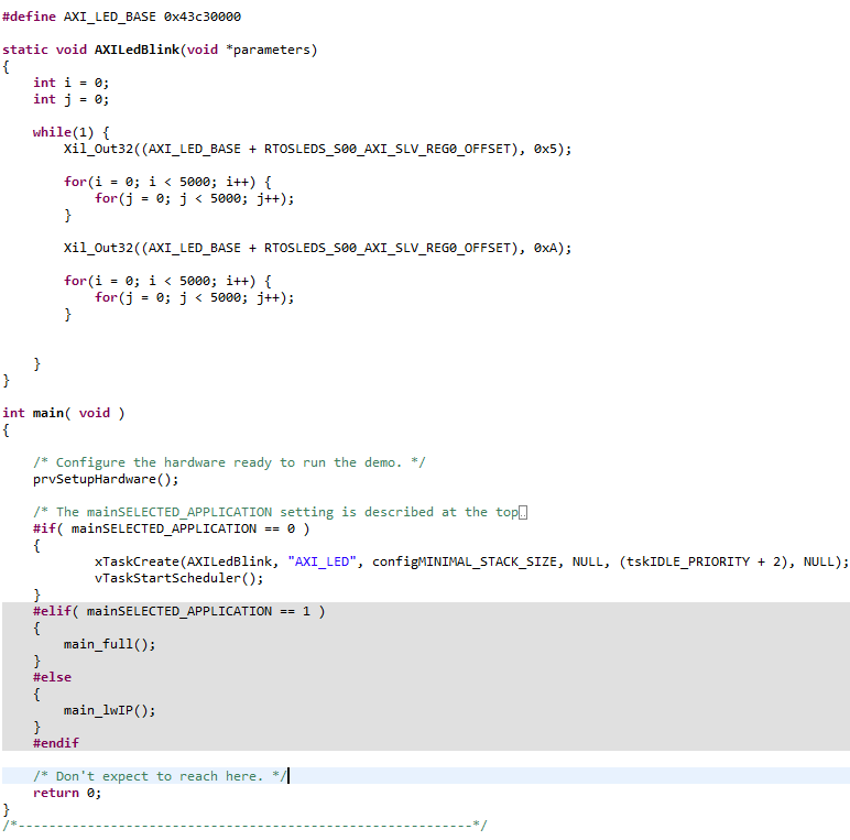
13. To test it all out i created a simple task that would send the data 0x5, 0xA alternately after a fixed delay to the AXI peripheral thereby displaying the pattern on the zybo leds.


14. The last step is the comment out the call to vParTestInitialise() from the prvSetupHardware function as it is not related to the Zybo board.

15. Well, after the above steps, if everything compiles correctly without errors, program the FPGA and the ELF using the Xilinx Tools menu and start the debug session. Make sure you have the Zybo powered up from the wall adapter and the JP5 header set to JTAG. In my case the USB power did not work as the level shifters were not enabled when i used it.

FreeRTOS on the Digilent Zybo....done...

The entire project on GitHub: 

My other FreeRTOS adventures:


Thursday, February 26, 2015

Samsung S-Pen Internals

The S Pen, introduced with the Galaxy Note, is faster and more accurate than conventional stylus pens. It is an input tool that provides a similar feel to an actual pen by detecting the pressure applied on the screen with great accuracy (wait, what....) [Source]

I was lucky to get my hands on a spare S Pen which turned out to be not so lucky for the pen. This post will explore the S Pen internals, crack it open, hook it up to a scope etc.

Cracking the Pen
The S Pen is a very robust design and it's internal circuitry cannot be easily accessed. You will have to use a saw or a dremel to carefully cut it open. I used a dremel to mercilessly slaughter the S Pen. The best position to start sawing would be at a distance of about 80 mm from the tip of the pen. Then slowly working your way up towards the tip till you reach a printed circuit board capped with a small plastic holder as shown in the images below. The pcb assembly slides outwards away from the tip. You will have to remove the plastic button in order to remove the pcb effortlessly.


The S Pen disassembled. Top PCB and bottom side

A close up of the components on the pcb is shown below. Starting from the tip we have the coil assembly consisting of a 0.22 mm dia (approx.) wire wound on a soft iron core which is not cylindrical. The tip is connected to a spring at the base of the assembly which appears to be some kind of switch or a variable capacitor. I believe this assembly consisting of the spring deals with the pressure sensing, either by bringing the coil close to the display surface by compressing the spring or by using the contacts at the base of the assembly as a variable parallel plate capacitor. We then have the push button that is usually used for the air command interface followed by two sensitivity adjustment potentiometers and a bunch of capacitors connected in parallel to the coil thereby forming an LC resonant circuit. The little solder blobs below each capacitor are jumper connections. Therefore as shown below, from left to right the first capacitor and the last capacitor are not connected in parallel with the coil. If you are wondering where is the circuit diagram.....it's coming soon....

Close up of the PCB


Operating Principle

Samsung partnered with Wacom to develop the S Pen. The pen works on the principle of Electro-Magnetic Resonance (EMR). Devices utilizing EMR Technology do not require any cable or built-in battery-based power supply at all. This is because the cellphone incorporates a sensor board beneath the OLED display that detects the pen's movement. Weak energy is induced in the pen's resonant circuit by a magnetic field generated by the sensor board surface. The pen's resonant circuit then makes use of this energy to return a magnetic signal to the sensor board surface. By repeating this movement, the board detects information on the pen's coordinate position and angle, as well as on its general operating condition including speed and writing pressure, etc. A sensor unit is equipped at the side of the sensor board to switch the magnetic field on and off and to receive signals at high speed and detect various kinds of information. In principle, all Wacom's tablet devices are composed of this kind of sensor unit and electronic pen. In addition, the sensor unit itself consists of a sensor board and a control board.

The sensor board is an array of tiny loop antennas arranged in overlapping X and Y directions. The control board switches a high frequency signal into each of the loop antenna coils. This causes them to generate a magnetic field. When the pen passes through this magnetic field, it picks up and stores energy in it's resonant circuit. The control board then instantaneously switches to the receiver and roughly determines the pen's location by scanning all the loop coils. After that, the control board scans multiple loop coils in the vicinity of the pen, and uses the information to calculate the pen's coordinate value precisely. The control board has its own custom DSP circuit performing all the high speed calculations.

For example, let's take the Samsung Galaxy Note 2. The internal view of the Note is shown below. Notice the golden panel. That is the sensor board - the digitizer that interacts with the S Pen [Source]


Hooking it Up

In order to see what is going on inside the S Pen circuitry i connected some wires to the coil pads on the pcb and hooked it up to my oscilloscope. The device operates at a certain carrier frequency as shown below. The signal is power optimized and the data transaction is in some frames that i observed in a repetitive pattern. The same pattern seems to shape-shift when the S Pen is oriented to the display at different angles.Refer to the text below each image for more information. The scope waveform was very jumpy and the values mentioned are close approximate readings off the scope.


Each frame is approximately 15 ms. The above pattern repeats over and over.


Here is the same 15 ms frame but it appears different because the pen was oriented at an angle of around 30 degrees (back end towards the home key) with the surface of the display


Here is the same 15 ms frame but now oriented at an angle of around 120 degrees (back end away from home key) with the surface of the display


Let's turn that time base down


The carrier frequency appears to be approximately 560 KHz


The FFT of the signal gives a strong peak around 560 KHz


Wonder what happens when you push the small button on the S Pen ? The 560 KHz peak shifts to 530 KHz. I guess this frequency shift gets detected as a button press by the sensor board. Pressing the switch must be connecting additional capacitance in the LC parallel circuit thereby changing its resonant frequency. Barely noticeable in the image, but if you click on the image and switch to the image viewer you can alternate between image numbers 8 and 9 using the arrow keys to observe the shift.


This is the frequency response of the LC parallel resonant circuit of the S Pen which was obtained by sweeping a sine wave from 100 KHz to 1 MHz at the coil terminals, with the coil connected to the PCB. The dip is at around 565 KHz.

In a nutshell, the phone containing the "digitizer" or sensor board generates a magnetic field that induces a current in the coil that is connected to the parallel LC tank circuit, the sensor board then switches into receiving mode, letting the resonant energy drain through the S Pen coil thereby detecting it's position, pressure and angle. 

Let's  go back to the first paragraph of this post referenced from another post stating "detecting the pressure applied on the screen". Well, nope. The statement is framed incorrectly leading anyone to believe there are pressure sensors on the screen for the S Pen. But as we found out, it is not so...

The S Pen therefore accomplishes a lot with simple circuitry and basic principles of electromagnetism. Michael Faraday will be proud :P

These observations are based on the S Pen i own using the Digilent Analog Discovery. If you perform the same set of experiments and get to know something new and weird or decode the frame structure if any, comment below. Found a mistake in the text ? comment below...

For information on LC resonant circuits check out the video below:


Sunday, February 1, 2015

Short Circuit - Part 1

I've  got my hands on the Zumo 1.2 robot and it's time to do some crazy stuff with it. Last month i finished designing a customized baseboard for the Teensy 3.1 Cortex-M4 board by PJRC. This baseboard was tailored specifically for the Zumo. More details on the Zumo 1.2 can be found here. The zumo is designed such that it acts as a shield for the arduino uno board. However if you mount the standard original arduino on the zumo, you cannot mount other shelds. Some pins are specific to the Zumo which you can check on the Zumo wiki. Some of my friends who are founders of Entesla managed to give me one of their arduino clones - the Entuino with all the headers removed. I soldered the new headers as per my convienience, removed the DC jack and reset switch and it looks like this.


When mounted on the Zumo the board looks like this. Now i can mount an infinite number shields on top of this board (conditions apply....even mathematically :P)


Notice that few of the pins have been cut off such that they do not interfere with the shield on top. These are primarily the controls for the zumo motors that were mapped to the same pins used by SPI. The power pins too were not made available to shields above the entuino. The Teensy board has its own voltage regulators for 5V and 3.3 V and hence sources from the Vin supply from the Zumo shield which is 7.5 V


I will be using the arduino for the sole purpose of controlling the motors. All the sensors' data computation will be taken care by the Teensy over the I2C bus. The teensy and entuino communicate with each other via the hardware UARTs, (0, 1) on the entuino and (0,1) Serial1 on the Teensy. The Teensy also has a NRF24L01+ interfaced over the SPI bus for remotely controlling the bot and for data telemetry. The Teensy base board also has support for the ESP8266 wifi (not connected) and a 40 pin header to connect the Raspberry Pi. The Teesny baseboard and the RPi communicate over the UART. The whole block diagram of the entire system is shown below. Currently the ESP8266 and RPi are not connected to the teensy baseboard. Initially i had planned to use the SoftwareSerial library on the teensy for comms between teensy and entuino, but that backfired as the SoftSerial library is defunct. Therefore, i patched the ESP uart to the hardware uart of the entuino (the white wires in pics below).


The fully assembled robot.


The two boards


Now i have to take utmost care to solder the 40 pin header whose component side is behind the board. R.I.P ESP8266. #facepalm, softwareserial #fail.


The Eagle schematic. Not perfect i must say, jeez, look at some vias and those clearances... :P


Fully Powered Up


More adventures with this in Short Circuit - Part 2.

Tuesday, July 8, 2014

Visible Light Communications

My experiments with Visible Light Communication can be found here. Most of the circuit components are selected according to their easy availability in my geographical area without spending too much on shipping (seriously a photodiode from Digikey is 1.5 USD + 60 USD shipping !!! ).

All of this can act as a reference for someone in designing a VLC system or atleast act as a guide on how to evaluate sensors etc. Of course sensors may vary but the workflow would somewhat remain the same...

Stage I
Stage One is all about figuring out if i have the right sensors for the job. A sensor with fast rise and fall times and a fast MOSFET based LED driver. Level: Basic


 Stage II


Visible Light Communication Chronicles Part III

Welcome to Part 3 of my experiments with visible light communication. In this post i will reveal the final circuit that i used for transmitting UART data over the link. Alternatively i also managed a successful Manchester encoded data transmission over the VLC link. The circuits for the transmitter and receiver are shown below. This is the most basic configuration and yields a maximum UART data transmission rate of 2400 Baud (with flicker) and transmission of Manchester encoded data stream at 1200 Baud (no flicker).

The transmitter above consists of a P55NF06 N-Channel MOSFET whose gate is driven by one of the Arduino pins. The data stream is directly connected to the gate. This causes variations in the drain to source current and varies the drain source voltage Vds and hence the intensity of the LED. This circuit just acts as a modulator. VDD is kept at 13 Volts and in the ON state the LED draws approximately 0.87 A. In the next iteration of this circuit i plan to buffer the gate input and also add a gate driver for a faster response. The code on the transmitter side is hown below. This is the Manchester encoded data stream using the Manchester library for Arduino that you can find here. The test code is pretty basic and just transmits a string of data. As a homework you've got to figure out other parts of the code yourself. No freebies !! Same goes for most circuits.


As mentioned in earlier posts the receiver consists of a TEMT 6000 ambient light sensor whose output is coupled through a capacitor into a LM324N based non-inverting comparator. The reference voltage to the comparator is selectable between 2.5V and 3.3V. This determines how accurately the signal is re-constructed. The output of the OP-AMP is then connected to an Arduino pin as input via a buffer. The various signals are shown below. The power rails of the LM324N quad are connected to 5V and GND.


The output of the TEMT 6000 is in orange. This signal is fed into the OP-AMP non-inverting input. Observe the non-linearity due to the fall time. This is the signal for a Manchester encoded data at 1200 baud. The signal in blue color is the output of the comparator. Based on the reference voltage set the timing of the manchester data stream is not affected and can be decoded easily.


In the above case i reduced the drain-source voltage Vds to around 8V thereby reducing the intensity of light. Observe the non-linearity in both the rise and fall-times of the TEMT 6000 sensor. However the comparator was successfully able to re-construct the signal. The code on the receiver side is shown below


The plots for UART data are shown below. The first plot is the UART data at 2400 Baud with Vds = 13V. The second plot is the same data at 2400 Baud but with Vds = 8V. Note the effects of LED brightness on the output of the sensor. The orange plot is the sensor output and the blue plot is the comparator output. The dark black horizontal line is Vref at 2.5V.


Complete loss of timing information in this one

This concludes the initial stages of experimentation for the visible light communication link that i want to build. The primary objective right now is to find a high speed sensor whose rise and fall times are in the nanosecond range. Less than or equal to 100 ns preferably. Once i get my hands on the new sensor i will post the details about it here. Until then, take it easy.....


Friday, July 4, 2014

Visible Light Communication Chronicles Part II


This is the continuation from Part I on my experiments with visible light communication that i posted sometime ago here. I set up a basic transmitter - receiver circuit, a square wave was given as an input to the transmitter and the output of the reciever was monitored. The transmitter consisted of a N-channel power MOSFET - P55NF06 driving a LED and the receiver consisted of the TEMT 6000 ambient light sensor. The square wave signal was generated using an Arduino MEGA and all the I/O signals were monitored using the Digilent Analog Discovery. Why i chose the above mentioned MOSFET ? because i already had it in stock and decided to use it. The light source is a commercially available 10 W high power LED which i got over here.

Transmitter

The overall circuit is shown below. The gate of the MOSFET is driven by one of the arduino pins. The sketch on the arduino is nothing but the blinky sketch. By adjusting the parameters to the delay function i could generate a square wave from 2 KHz (delay(1)) to 0.5 Hz (delay(1000). The gate resistors Rs and Rg were chosen such thar R1 << R2. From the datasheet, the P55NF06 N-channel mosfet has a drain-source voltage of 60V and a max drain current of 50A.The gate threshold voltage is around 2-4V. The LED forward voltage is around 7V. When turned ON the LED draws approximately 0.5 A which is within the spec of the MOSFET. The transmitter is assembled on a breadboard (yeah kind of not a good choice for a circuit like this, specially considering the mosfet parasitics, you never know...)


Receiver:

The receiver consists of the TEMT 6000 breakout board powered via a 3.3 V supply and it's output fed into the analog discovery. 

The distance between the RXR and TXR is 6 cm. I kept it small for initial measurements. All the signals seen on the scope of the analog discovery are shown below.


The above square wave has a time period of  2 seconds, 0.5 Hz. The blue signal is the input signal and the orange signal has been captured at the output of the ambient light sensor. Note that the rise time and fall time of both the signals appear to be instantaeneous. Also note that when the LED is OFF the TEMT sensor output does not drop to zero but goes to around 48 mV which as i mentioned in an earlier post is the interference from the fluorescent light in my room. The interference is visible in the above image when the input signal is 0V.


The input signal here is of 5 Hz. The output of the ambient light sensor follows the input given to the MOSFET. Note the ripple in the output when input goes to 0V.


In this case the input signal is of 50 Hz. Notice that the output signal starts exhibiting some non-linearity when the MOSFET turns OFF. The interference due to the fluorescent light starts getting negligible. More on this a scroll later.


In this case the input signal has a frequency of 500 Hz. If we continue to increase the frequency the signal at the output of the TEMT 6000 almost disappears and all we get is a DC voltage. with very faint signs of the input signal. After this initial test i decided to give the output of the UART to the TXR circuit and observe the output on the TEMT 6000. Here are the output response of the light sensor to different baud rates


300 Baud.


600 Baud. OFF time non-linearity starts kicking in.


2400 Baud.


4800 Baud. A still noticeable signal that can be recovered using some extra circuitry.


9600 Baud. Beyond 9600 you can only imagine what will happen to the signal at the sensor output.

To investigate on the TXR side. I used a 5V drain-source supply and switched the MOSFET using a 500 Hz gate signal. The following image shows the scope output. The output (orange) was taken at the drain hence the signal inversion. It can be seen that when the gate voltage drops to 0V, turning off the mosfet, the output voltage increases non-linearly with time.(based on the mosfet turn-off delay parameters). The delta is 46.7 usec. The datasheet says that the turn-off delay is around 30 nsec for the specified test conditions.


Allrighty that is a lot of information in this post. Part 3 of this series will elaborate on the analysis of the circuit, MOSFET parameters and the above plots.  Until then, take it easy...

Update

I did one more test in which i plotted the TEMT6000 output over the drain-source voltage Vds.


The orange plot is the output of the light sensor and the blue plot is Vds, which is inverted as i connected the scope to the drain as shown in the schematic. The nonlinearity that i had seen before was therefore confirmed to be due to the TEMTP 6000 sensor. I did a couple of tests with varying input frequencies and found that in all cases the time it took for the sensor outout to go from maximum to 0V was 1.4 msec.which means that it can handle signals from 1 Hz to 714 Hz approximately. This was true as seen in the output plots above. Increasing the Vcc for the sensor to 5V does not help. Time to find a better sendor or fix the output of this one. I will probably have to make a new board and change the 10K resistor to a more feasible value.