Saturday, April 4, 2015

FreeRTOS on Xilinx Zynq Zybo [Single Core]

This post will guide you in getting FreeRTOS up and running on the Zybo Zynq 7000 development board from Digilent. The post will focus on running FreeRTOS on a single core. After a few eons i shall be putting up another post on running FreeRTOS, each on one core. The entire project has been uploaded to Git and the link is somewhere down below.

What we are going to do ?
1. Create a custom AXI4 Lite peripheral whose output port will be connected to the four LEDs on the Zybo.

2. Get FreeRTOS to run on the ZYBO.

3. Create a task in FreeRTOS to write data to the AXI peripheral and display it on the LEDs.

Pre-requisites:
1. The Zybo board.
2. Latest FreeRTOS source code.
3. Vivado 2014.x and Xilinx SDK 2014.x.
4. Knowledge of using the Xilinx tools.

Steps:
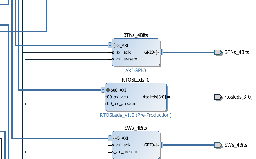
1. The first step is to build and setup  the hardware in Vivado. To keep this post short i would recommend you to click here and follow the Embedded Linux Tutorial by Digilent. You only need to refer this post on how to create a AXI Lite peripheral, section 1 - Hardware Customization and generate the Bitstream. It's upto you to work in VHDL or Verilog. I know VHDL therefore i had to delete the system_wrapper, change the Project Settings and regenerate the system_wrapper and other code in VHDL. Here is my custom AXI 4 LITE peripheral - RTOSLeds_0. Make sure that you assign address to your peripheral in the Address Editor before generating the bitstream.



2. Once you've finished generating the bitstream export it and Launch the SDK.

3. Within the SDK create a new application project, preferably a blank one or the HelloWorld project.
This should generate the BSP and the hello world project files. Now since we will not be using the helloworld.c file, we can delete it. Additionally remove the helloworld reference from the Makefile (that's if you created a helloworld project instead of a empty one).

4. On the FreeRTOS website there is a page that describes porting it to the Zynq processor. You will find the same project at this path in your FreeRTOS directory - \FreeRTOSV8.2.1\FreeRTOS\Demo\CORTEX_A9_Zynq_ZC702. The platform and BSP in that folder are not for the Zybo board therefore we do not need to refer those folders at all since we have created our own hardware and bsp in the steps above.

5. The  RTOSDemo folder which is our folder of interest contains the necessary files that need to be imported to our project workspace. Not all files, just a few that are highlighted below. The platform related files will already be present in the project.
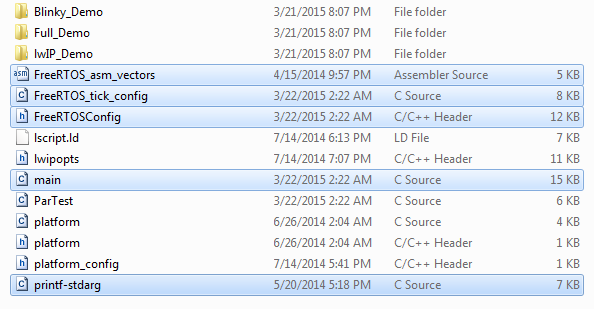
Copy the above highlighted files to the src folder of the sdk project.

6. Navigate to the - \FreeRTOSV8.2.1\FreeRTOS\Source\portable\GCC\ARM_CA9 folder and copy port.c, portASM.S and portmacro.h to the xilinx sdk src folder.

7. Navigate to the - \FreeRTOSV8.2.1\FreeRTOS\Source folder and copy all the six  C files to the project.

8. Copy the FreeRTOS headers from the include directory at the same path [7] into the xilinx sdk.

9. Copy  heap_4.c from the \FreeRTOSV8.2.1\FreeRTOS\Source\portable\MemMang directory into the project directory.

10. Your Xilinx SDK project src folder should now contains all the files as shown below.


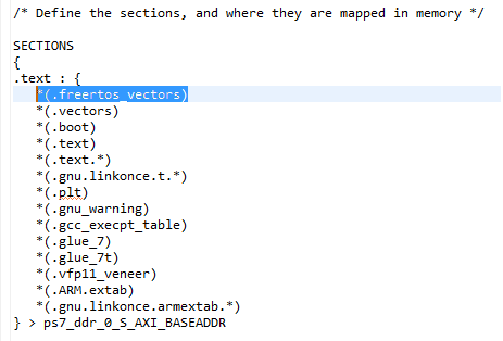
11. The next important thing that needs to be changed is the linker script file - lscript.ld. There is only one new line to be added here as highlighted below.


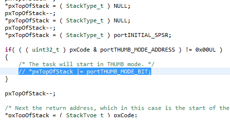
12. I do not want my code to run in thumb mode. Therefore i commented out the line shown below in the function pxPortInitialiseStack present in file port.c. In FreeRTOSConfig.h change the configCPU_CLOCK_HZ macro to 50Mhz.


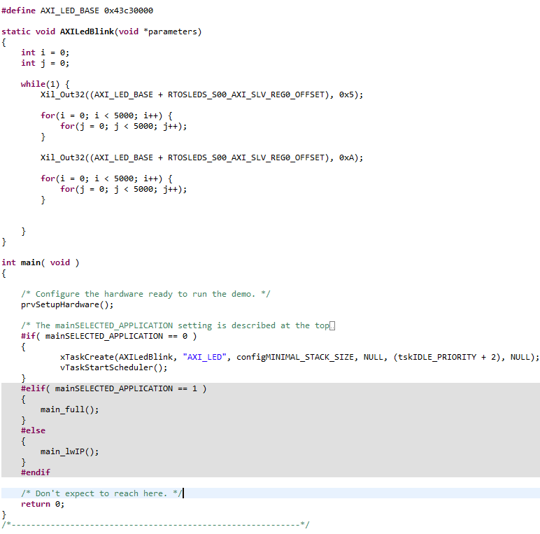
13. To test it all out i created a simple task that would send the data 0x5, 0xA alternately after a fixed delay to the AXI peripheral thereby displaying the pattern on the zybo leds.


14. The last step is the comment out the call to vParTestInitialise() from the prvSetupHardware function as it is not related to the Zybo board.

15. Well, after the above steps, if everything compiles correctly without errors, program the FPGA and the ELF using the Xilinx Tools menu and start the debug session. Make sure you have the Zybo powered up from the wall adapter and the JP5 header set to JTAG. In my case the USB power did not work as the level shifters were not enabled when i used it.

FreeRTOS on the Digilent Zybo....done...

The entire project on GitHub: 

My other FreeRTOS adventures:


Thursday, February 26, 2015

Samsung S-Pen Internals

The S Pen, introduced with the Galaxy Note, is faster and more accurate than conventional stylus pens. It is an input tool that provides a similar feel to an actual pen by detecting the pressure applied on the screen with great accuracy (wait, what....) [Source]

I was lucky to get my hands on a spare S Pen which turned out to be not so lucky for the pen. This post will explore the S Pen internals, crack it open, hook it up to a scope etc.

Cracking the Pen
The S Pen is a very robust design and it's internal circuitry cannot be easily accessed. You will have to use a saw or a dremel to carefully cut it open. I used a dremel to mercilessly slaughter the S Pen. The best position to start sawing would be at a distance of about 80 mm from the tip of the pen. Then slowly working your way up towards the tip till you reach a printed circuit board capped with a small plastic holder as shown in the images below. The pcb assembly slides outwards away from the tip. You will have to remove the plastic button in order to remove the pcb effortlessly.


The S Pen disassembled. Top PCB and bottom side

A close up of the components on the pcb is shown below. Starting from the tip we have the coil assembly consisting of a 0.22 mm dia (approx.) wire wound on a soft iron core which is not cylindrical. The tip is connected to a spring at the base of the assembly which appears to be some kind of switch or a variable capacitor. I believe this assembly consisting of the spring deals with the pressure sensing, either by bringing the coil close to the display surface by compressing the spring or by using the contacts at the base of the assembly as a variable parallel plate capacitor. We then have the push button that is usually used for the air command interface followed by two sensitivity adjustment potentiometers and a bunch of capacitors connected in parallel to the coil thereby forming an LC resonant circuit. The little solder blobs below each capacitor are jumper connections. Therefore as shown below, from left to right the first capacitor and the last capacitor are not connected in parallel with the coil. If you are wondering where is the circuit diagram.....it's coming soon....

Close up of the PCB


Operating Principle

Samsung partnered with Wacom to develop the S Pen. The pen works on the principle of Electro-Magnetic Resonance (EMR). Devices utilizing EMR Technology do not require any cable or built-in battery-based power supply at all. This is because the cellphone incorporates a sensor board beneath the OLED display that detects the pen's movement. Weak energy is induced in the pen's resonant circuit by a magnetic field generated by the sensor board surface. The pen's resonant circuit then makes use of this energy to return a magnetic signal to the sensor board surface. By repeating this movement, the board detects information on the pen's coordinate position and angle, as well as on its general operating condition including speed and writing pressure, etc. A sensor unit is equipped at the side of the sensor board to switch the magnetic field on and off and to receive signals at high speed and detect various kinds of information. In principle, all Wacom's tablet devices are composed of this kind of sensor unit and electronic pen. In addition, the sensor unit itself consists of a sensor board and a control board.

The sensor board is an array of tiny loop antennas arranged in overlapping X and Y directions. The control board switches a high frequency signal into each of the loop antenna coils. This causes them to generate a magnetic field. When the pen passes through this magnetic field, it picks up and stores energy in it's resonant circuit. The control board then instantaneously switches to the receiver and roughly determines the pen's location by scanning all the loop coils. After that, the control board scans multiple loop coils in the vicinity of the pen, and uses the information to calculate the pen's coordinate value precisely. The control board has its own custom DSP circuit performing all the high speed calculations.

For example, let's take the Samsung Galaxy Note 2. The internal view of the Note is shown below. Notice the golden panel. That is the sensor board - the digitizer that interacts with the S Pen [Source]


Hooking it Up

In order to see what is going on inside the S Pen circuitry i connected some wires to the coil pads on the pcb and hooked it up to my oscilloscope. The device operates at a certain carrier frequency as shown below. The signal is power optimized and the data transaction is in some frames that i observed in a repetitive pattern. The same pattern seems to shape-shift when the S Pen is oriented to the display at different angles.Refer to the text below each image for more information. The scope waveform was very jumpy and the values mentioned are close approximate readings off the scope.


Each frame is approximately 15 ms. The above pattern repeats over and over.


Here is the same 15 ms frame but it appears different because the pen was oriented at an angle of around 30 degrees (back end towards the home key) with the surface of the display


Here is the same 15 ms frame but now oriented at an angle of around 120 degrees (back end away from home key) with the surface of the display


Let's turn that time base down


The carrier frequency appears to be approximately 560 KHz


The FFT of the signal gives a strong peak around 560 KHz


Wonder what happens when you push the small button on the S Pen ? The 560 KHz peak shifts to 530 KHz. I guess this frequency shift gets detected as a button press by the sensor board. Pressing the switch must be connecting additional capacitance in the LC parallel circuit thereby changing its resonant frequency. Barely noticeable in the image, but if you click on the image and switch to the image viewer you can alternate between image numbers 8 and 9 using the arrow keys to observe the shift.


This is the frequency response of the LC parallel resonant circuit of the S Pen which was obtained by sweeping a sine wave from 100 KHz to 1 MHz at the coil terminals, with the coil connected to the PCB. The dip is at around 565 KHz.

In a nutshell, the phone containing the "digitizer" or sensor board generates a magnetic field that induces a current in the coil that is connected to the parallel LC tank circuit, the sensor board then switches into receiving mode, letting the resonant energy drain through the S Pen coil thereby detecting it's position, pressure and angle. 

Let's  go back to the first paragraph of this post referenced from another post stating "detecting the pressure applied on the screen". Well, nope. The statement is framed incorrectly leading anyone to believe there are pressure sensors on the screen for the S Pen. But as we found out, it is not so...

The S Pen therefore accomplishes a lot with simple circuitry and basic principles of electromagnetism. Michael Faraday will be proud :P

These observations are based on the S Pen i own using the Digilent Analog Discovery. If you perform the same set of experiments and get to know something new and weird or decode the frame structure if any, comment below. Found a mistake in the text ? comment below...

For information on LC resonant circuits check out the video below: