Showing posts with label franklin. Show all posts

Friday, July 22, 2016

ARM FastModels - Part 1 - The SoC

The ARM FastModels series of posts will be focusing on building a simple SoC from scratch, bringing up FreeRTOS on the SoC, creating a custom IP using the native language LISA and porting of the SMSC91C111 Ethernet controller driver on the virtual platform. The links to each of the below topics will be enabled once the post is ready for hosting.

  • 1. The SoC hardware architecture.
  • 2. Bringing up Free RTOS on the SoC.
  • 3. Adding a custom peripheral IP.
  • 4. Porting the Network Controller driver.

I have been playing around with FastModels for quiet some time and it is a fascinating tool to design and build your own SoC Virtual Prototype from scratch and learn the process of interfacing various IPs to the SoC. More information on FastModels can be found here. It is available for a 30 day trial for a processor of your choice. I chose the Cortex-A5 MPCore processor and therefore the SoC will be designed around it. Using the tool-chain is pretty basic and can be almost easily followed through using the available user guides. Remember i said 'almost'. Most advanced features and IPs are not well documented or are proprietary and it could give you a concussion if you try to interface them.

If you are running on Windows then you need a full version of Visual Studio 2013 to compile the simulation ISIM executable. On Linux you can use the freely available gcc 4.8 compiler. I am using FastModels 10 on a Windows machine with a VS2013 60-day trial.

For my SoC code-named RAVEN i decided to go for a simple hardware architecture that consisted of a Cortex A5 Quad Core processor clocked at 500 MHz, PL011 UART IP, 1GB of RAM, SMSC91C111 Ethernet controller. This being a simulation, not all core features are available. To check out the features that are available for the Cortex A5MPCore model view the DUI0834H Fast Models reference manual section 3.2.15.

The Cortex-A5 model can provide full functional simulation of the ARM v7 architecture and comes bundled with the SCU, GIC, Private timer and WDT per core, one Global Timer and an Advanced Coherency Port. You can refer the A5 MPCore reference manual here.

The FastModels design environment is a code based and block design based IDE akin to a Visual Programming IDE where you can drag and drop various IPs and connect them. If you have used tools like Xilinx Vivado or Multisim bob's your uncle. The scripting language is called LISA and is similar to C++. 


The final SoC is shown above. Starting from the left -

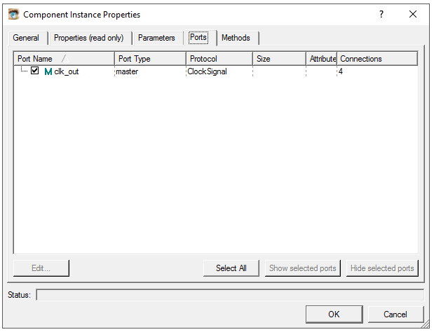
XTAL: The Master Clock IP. a clock signal of 1 Hz is available at the clk_out port of this IP. The clk_out master port follows the ClockSignal protocol and can only be connected to another IP that has a port e.g. clk_in declared as a slave port with ClockSignal protocol. A list of available protocols is in the reference manual. To view the IP properties, right click the IP block and select Object Properties which brings up the following dialog box.


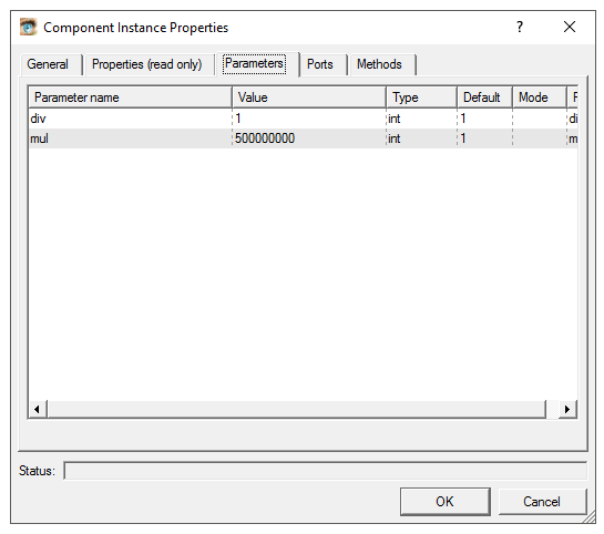
CORE_CLK: This is a Clock Divider IP. This IP can either multiply or divide the clock frequency that is input at its clk_in terminal. The new clock signal comes out of the clk_out signal. This IP has been used to provide the clock frequency for the Cortex-A5. As shown below the mul parameter of this IP is 500000000. Since the input to the divider is 1 Hz it is multiplied by 500000000 to give a frequency of 500 MHz.This output is connected to the clk_in port of the processor.

PERIPHERAL_CLK: This is again a Clock Divider with the mul parameter set to 166666666 i.e. 166.66 MHz. FastModels provide a functionally accurate simulation of the system and not a timing accurate hence these clock values seldom do not influence functional verification. However, according to the datasheet the peripheral clock must be an integral multiple [N] of the core clock period with the multiple being greater than or equal to 2. Given a 500 MHz clock with 2ns period selecting N = 3 gives a 3:1 ratio and the peripheral clock period as 6ns hence 166.66 MHz.

UART_CLK and ETHERNET_CLK: The clock dividers for the UART and ETHERNET IPs clocked at 15MHz and 25 MHz respectively.

BUSDECODER0: The bus decoder IP is responsible of routing the bus transactions to the respective slave devices on the bus.The transactions on the PVBus are similar to AXI transactions. As shown, this IP is connected to the pvbus_m port of the processor which is one of the MASTER AXI ports. Each of the slave interfaces on the pvbus_m_range master port must be configured with a base address and size of the slave peripheral which must be 4KB aligned. This forms the memory map for the peripherals as shown below.


Now then, i figured that it is just impossible to type everything in here. The best thing would be to demonstrate the entire design process. Here is the video of the SoC design in action !!


After the build is successful a isim executable will be created in a release/debug directory inside the project folder. This executable needs to be imported into DS-5 to run the software and for simulations.


Saturday, February 13, 2016

The Collatz Conjecture - Part 1


The Collatz Conjecture can be summarized as follows - Take any positive integer n. If n is even, divide it by 2 to get n / 2. If n is odd, multiply it by 3 and add 1 to obtain 3n + 1. Repeat the process indefinitely. The conjecture is that no matter what number you start with, you will always eventually reach 1. The property has also been called oneness - Wikipedia

So, for starters, i decided to write a program that will compute the Collatz sequence for a 64 bit number i.e. from 0 to 18,446,744,073,709,551,615 which equals 264 − 1. After reaching the end of the cycle for a given number the program prints out the number N and the length of the cycle S. However, it does not print every cycle length, it only prints the next cycle that is greater than the previously computed cycle length.


The above code was compiled using gcc with full optimization. The executable was run on a 3.0 GHz Core i7 Quad with 8 GB RAM. The process priority was changed to SCHED_RR using the chrt command. It took the machine two weeks to generate the output shown below. The largest cycle sequence we were able to compute was 1428 for the 13 digit number shown. In the next part of this article i shall be posting details about running the same code on my NVidia GPU using CUDA along with some insane optimizations.


Oh, and there is also a short-film on the Collatz Conjecture...


Friday, February 12, 2016

Quadcopter Chronicles - I

So, i've decided to build my own drone from scratch. Here is a picture of the work in progress. The orange PLA chassis was printed on my 3D printer. It is going to be similar to the Crazyflie with a few modifications. So, why not buy the Crazyflie ? well, no fun in that...

So this is the X configuration. The slits have been cut into the motor housing to account for the error in the print caused by the 3D printer. I've observed with my printer that, if i give the hole diameter as 7.03 mm it always turns out to be less by around 0.2-0.1 mm, which is the error. When this happens the motors do not pass through the hole and i have to sit and file it which results in inconsistencies in the 4 holes.

By giving the same value of 7.03 mm is the diameter of the motor and a slit the motors can be accommodated in a tight fit by wedging the slit to allow the motors to pass though, removing the wedge causes the structure to wrap tightly around the motor due to it's elastic nature. 

Also there is something weird in the image below. If you figure it out leave a comment.


The body was designed in SolidWorks as shown below and weighs 9 grams. Yep, that is a lot of green, almost a relation fest, but i am learning to clean that up. Most of it is the symmetry relation due to mirroring the entities.


The motors and props are similar to the one used in the Crazyflie. The next task is to design the control system electronics.


If you would like to download the 3D STL model visit my Thingiverse link below:
http://www.thingiverse.com/thing:1336837

Licensed under Creative Commons


Thursday, June 18, 2015

FreeRTOS on Cortex-A8 FVP ARM DS-5

Here is an implementation of the FreeRTOS ARM Cortex-A port on the DS-5 Cortex-A8 Fixed Virtual Platform. I was planning to do this since a long time (as my beagleboard went up in magic smoke and i did not have any platform to experiment on) and now that it is finally done, you can evaluate FreeRTOS on a Cortex-A series processor without the need to purchase additional hardware. Students and professionals can also explore RTOS concepts / design methodologies or even tweak the OS, try real nasty things. This implementation is now available at my GitHub.

I am unaware of existing FVP implementations. I could not find any by doing a Google search. Hence, if you are aware of any such implementation please link in the comments below. Compiled and tested in ARM DS-5 Ultimate Edition (Evaluation) Version: 5.21.0 Build number: 5210017

Most of the information can be figured out by going through the code, by doing a diff of the source file with the original, however some brief implementation details are mentioned below.

Keep this document handy as it contains the memory map of the FVP. Also note that this is a simulation and will not be "real-time". This project is only to understand the inner workings of FreeRTOS or any RTOS in general. To run it on real hardware you will still need the board specific settings. For that refer to my earlier post on FreeRTOS with the BeagleBoard. Turn on Rate-Limit in the CLCD screen for stable response if required.

Import this project into DS-5. Compile and create a Debug Configuration for the Cortex-A8 FVP Bare-Metal debug.

The system is configured for a maximum 32 interrupts. The FVP has 64 interrupt sources out of which the first 16 are SGIs. More information on interrupt priority assignments on Cortex-A series specific to this OS can be found here.

I am using the SP804 Timer Module 0 to generate the tick interval. The timer is configured as a 32-bit counter, periodic timer. timer_init.s has a minimal assembly implementation.

The port for the Cortex-A series can be found in the FreeRTOS portable directory - \FreeRTOSV8.2.1\FreeRTOS\Source\portable\RVDS\ARM_CA9.

configCPU_CLOCK_HZ and configPERIPHERAL_CLOCK_HZ would really not matter in the simulation. The tick timer has been configured with a value of 0x3e8. The FreeRTOSConfig.h file has been used by modifying the one in Renesas demo project.

As this will be running on a Cortex-A8 FVP, the Cortex-A8 startup file can be found in the bare-metal examples directory in the DS-5 installation. This file has been modified for the current implementation by adding stack initialization, enabling GIC etc.

Additional changes in port.c for handling the tick and setting API for clearing the timer interrupt.

main.c implements 3 tasks for demonstration:
RollingLEDSTask - This task nudges the LEDs in the CLCD window one at a time, prints the number of times it's called and goes to sleep for 1 tick.

PrintHelloTask - Prints hello world to the console and the number of times it is called and goes to sleep for 5 ticks.

PrintKeyboardTask - I was looking for a method to externally trigger events in the DS-5 debugger. Unfortunately the GPIO controller in the FVP lacks this capability. Therefore the only method was to use the PL050 implementation in the FVP to trigger events using the keyboard connected to the computer :P

PL050.c therefore contains a minimal implementation of the driver for this FVP peripheral. the PrintKeyboardTask blocks on a semaphore on start up. If a key is pressed on the keyboard while the CLCD window is active, the PL050 generates 3 interrupts. The 3 bytes sent in sequence are [scancode], [0xF0], [scancode] Leave a comment below if you know why 3 bytes. The first byte is indeed the scan-code but i have no idea what the second byte is. Ideally it should be the shift key status. On the third interrupt the semaphore is released from the IRQ handler of the peripheral which activates the task to print out to the console. To get the ascii value of the key, you might have to convert the scancode to the corresponding ascii value. For character - a, i was getting scan code of 0x1C which might differ based on your locale / keyboard type.

P.S: Most files are in assembly and not in C e.g the timer and GIC APIs, the reason being - i already had these ready from earlier projects, hence used the same. You can use your own implementation in C if you require. 

To enable FreeRTOS awareness in DS-5 please enable the flags mentioned in this article on ARM Infocenter.

If you have any questions leave a comment below. Few screenshots of my tool settings are shown below.


Available on FreeRTOS interactive site

http://interactive.freertos.org/entries/83853195-FreeRTOS-on-Cortex-A-FVP-ARM-DS-5