Showing posts with label arm. Show all posts

Friday, July 22, 2016

ARM FastModels - Part 1 - The SoC

The ARM FastModels series of posts will be focusing on building a simple SoC from scratch, bringing up FreeRTOS on the SoC, creating a custom IP using the native language LISA and porting of the SMSC91C111 Ethernet controller driver on the virtual platform. The links to each of the below topics will be enabled once the post is ready for hosting.

  • 1. The SoC hardware architecture.
  • 2. Bringing up Free RTOS on the SoC.
  • 3. Adding a custom peripheral IP.
  • 4. Porting the Network Controller driver.

I have been playing around with FastModels for quiet some time and it is a fascinating tool to design and build your own SoC Virtual Prototype from scratch and learn the process of interfacing various IPs to the SoC. More information on FastModels can be found here. It is available for a 30 day trial for a processor of your choice. I chose the Cortex-A5 MPCore processor and therefore the SoC will be designed around it. Using the tool-chain is pretty basic and can be almost easily followed through using the available user guides. Remember i said 'almost'. Most advanced features and IPs are not well documented or are proprietary and it could give you a concussion if you try to interface them.

If you are running on Windows then you need a full version of Visual Studio 2013 to compile the simulation ISIM executable. On Linux you can use the freely available gcc 4.8 compiler. I am using FastModels 10 on a Windows machine with a VS2013 60-day trial.

For my SoC code-named RAVEN i decided to go for a simple hardware architecture that consisted of a Cortex A5 Quad Core processor clocked at 500 MHz, PL011 UART IP, 1GB of RAM, SMSC91C111 Ethernet controller. This being a simulation, not all core features are available. To check out the features that are available for the Cortex A5MPCore model view the DUI0834H Fast Models reference manual section 3.2.15.

The Cortex-A5 model can provide full functional simulation of the ARM v7 architecture and comes bundled with the SCU, GIC, Private timer and WDT per core, one Global Timer and an Advanced Coherency Port. You can refer the A5 MPCore reference manual here.

The FastModels design environment is a code based and block design based IDE akin to a Visual Programming IDE where you can drag and drop various IPs and connect them. If you have used tools like Xilinx Vivado or Multisim bob's your uncle. The scripting language is called LISA and is similar to C++. 


The final SoC is shown above. Starting from the left -

XTAL: The Master Clock IP. a clock signal of 1 Hz is available at the clk_out port of this IP. The clk_out master port follows the ClockSignal protocol and can only be connected to another IP that has a port e.g. clk_in declared as a slave port with ClockSignal protocol. A list of available protocols is in the reference manual. To view the IP properties, right click the IP block and select Object Properties which brings up the following dialog box.


CORE_CLK: This is a Clock Divider IP. This IP can either multiply or divide the clock frequency that is input at its clk_in terminal. The new clock signal comes out of the clk_out signal. This IP has been used to provide the clock frequency for the Cortex-A5. As shown below the mul parameter of this IP is 500000000. Since the input to the divider is 1 Hz it is multiplied by 500000000 to give a frequency of 500 MHz.This output is connected to the clk_in port of the processor.


PERIPHERAL_CLK: This is again a Clock Divider with the mul parameter set to 166666666 i.e. 166.66 MHz. FastModels provide a functionally accurate simulation of the system and not a timing accurate hence these clock values seldom do not influence functional verification. However, according to the datasheet the peripheral clock must be an integral multiple [N] of the core clock period with the multiple being greater than or equal to 2. Given a 500 MHz clock with 2ns period selecting N = 3 gives a 3:1 ratio and the peripheral clock period as 6ns hence 166.66 MHz.

UART_CLK and ETHERNET_CLK: The clock dividers for the UART and ETHERNET IPs clocked at 15MHz and 25 MHz respectively.

BUSDECODER0: The bus decoder IP is responsible of routing the bus transactions to the respective slave devices on the bus.The transactions on the PVBus are similar to AXI transactions. As shown, this IP is connected to the pvbus_m port of the processor which is one of the MASTER AXI ports. Each of the slave interfaces on the pvbus_m_range master port must be configured with a base address and size of the slave peripheral which must be 4KB aligned. This forms the memory map for the peripherals as shown below.


Now then, i figured that it is just impossible to type everything in here. The best thing would be to demonstrate the entire design process. Here is the video of the SoC design in action !!


After the build is successful a isim executable will be created in a release/debug directory inside the project folder. This executable needs to be imported into DS-5 to run the software and for simulations.


Thursday, June 18, 2015

FreeRTOS on Cortex-A8 FVP ARM DS-5

Here is an implementation of the FreeRTOS ARM Cortex-A port on the DS-5 Cortex-A8 Fixed Virtual Platform. I was planning to do this since a long time (as my beagleboard went up in magic smoke and i did not have any platform to experiment on) and now that it is finally done, you can evaluate FreeRTOS on a Cortex-A series processor without the need to purchase additional hardware. Students and professionals can also explore RTOS concepts / design methodologies or even tweak the OS, try real nasty things. This implementation is now available at my GitHub.

I am unaware of existing FVP implementations. I could not find any by doing a Google search. Hence, if you are aware of any such implementation please link in the comments below. Compiled and tested in ARM DS-5 Ultimate Edition (Evaluation) Version: 5.21.0 Build number: 5210017

Most of the information can be figured out by going through the code, by doing a diff of the source file with the original, however some brief implementation details are mentioned below.

Keep this document handy as it contains the memory map of the FVP. Also note that this is a simulation and will not be "real-time". This project is only to understand the inner workings of FreeRTOS or any RTOS in general. To run it on real hardware you will still need the board specific settings. For that refer to my earlier post on FreeRTOS with the BeagleBoard. Turn on Rate-Limit in the CLCD screen for stable response if required.

Import this project into DS-5. Compile and create a Debug Configuration for the Cortex-A8 FVP Bare-Metal debug.

The system is configured for a maximum 32 interrupts. The FVP has 64 interrupt sources out of which the first 16 are SGIs. More information on interrupt priority assignments on Cortex-A series specific to this OS can be found here.

I am using the SP804 Timer Module 0 to generate the tick interval. The timer is configured as a 32-bit counter, periodic timer. timer_init.s has a minimal assembly implementation.

The port for the Cortex-A series can be found in the FreeRTOS portable directory - \FreeRTOSV8.2.1\FreeRTOS\Source\portable\RVDS\ARM_CA9.

configCPU_CLOCK_HZ and configPERIPHERAL_CLOCK_HZ would really not matter in the simulation. The tick timer has been configured with a value of 0x3e8. The FreeRTOSConfig.h file has been used by modifying the one in Renesas demo project.

As this will be running on a Cortex-A8 FVP, the Cortex-A8 startup file can be found in the bare-metal examples directory in the DS-5 installation. This file has been modified for the current implementation by adding stack initialization, enabling GIC etc.

Additional changes in port.c for handling the tick and setting API for clearing the timer interrupt.

main.c implements 3 tasks for demonstration:
RollingLEDSTask - This task nudges the LEDs in the CLCD window one at a time, prints the number of times it's called and goes to sleep for 1 tick.

PrintHelloTask - Prints hello world to the console and the number of times it is called and goes to sleep for 5 ticks.

PrintKeyboardTask - I was looking for a method to externally trigger events in the DS-5 debugger. Unfortunately the GPIO controller in the FVP lacks this capability. Therefore the only method was to use the PL050 implementation in the FVP to trigger events using the keyboard connected to the computer :P

PL050.c therefore contains a minimal implementation of the driver for this FVP peripheral. the PrintKeyboardTask blocks on a semaphore on start up. If a key is pressed on the keyboard while the CLCD window is active, the PL050 generates 3 interrupts. The 3 bytes sent in sequence are [scancode], [0xF0], [scancode] Leave a comment below if you know why 3 bytes. The first byte is indeed the scan-code but i have no idea what the second byte is. Ideally it should be the shift key status. On the third interrupt the semaphore is released from the IRQ handler of the peripheral which activates the task to print out to the console. To get the ascii value of the key, you might have to convert the scancode to the corresponding ascii value. For character - a, i was getting scan code of 0x1C which might differ based on your locale / keyboard type.

P.S: Most files are in assembly and not in C e.g the timer and GIC APIs, the reason being - i already had these ready from earlier projects, hence used the same. You can use your own implementation in C if you require. 

To enable FreeRTOS awareness in DS-5 please enable the flags mentioned in this article on ARM Infocenter.

If you have any questions leave a comment below. Few screenshots of my tool settings are shown below.


Available on FreeRTOS interactive site

http://interactive.freertos.org/entries/83853195-FreeRTOS-on-Cortex-A-FVP-ARM-DS-5


Thursday, February 26, 2015

Samsung S-Pen Internals

The S Pen, introduced with the Galaxy Note, is faster and more accurate than conventional stylus pens. It is an input tool that provides a similar feel to an actual pen by detecting the pressure applied on the screen with great accuracy (wait, what....) [Source]

I was lucky to get my hands on a spare S Pen which turned out to be not so lucky for the pen. This post will explore the S Pen internals, crack it open, hook it up to a scope etc.

Cracking the Pen
The S Pen is a very robust design and it's internal circuitry cannot be easily accessed. You will have to use a saw or a dremel to carefully cut it open. I used a dremel to mercilessly slaughter the S Pen. The best position to start sawing would be at a distance of about 80 mm from the tip of the pen. Then slowly working your way up towards the tip till you reach a printed circuit board capped with a small plastic holder as shown in the images below. The pcb assembly slides outwards away from the tip. You will have to remove the plastic button in order to remove the pcb effortlessly.


The S Pen disassembled. Top PCB and bottom side

A close up of the components on the pcb is shown below. Starting from the tip we have the coil assembly consisting of a 0.22 mm dia (approx.) wire wound on a soft iron core which is not cylindrical. The tip is connected to a spring at the base of the assembly which appears to be some kind of switch or a variable capacitor. I believe this assembly consisting of the spring deals with the pressure sensing, either by bringing the coil close to the display surface by compressing the spring or by using the contacts at the base of the assembly as a variable parallel plate capacitor. We then have the push button that is usually used for the air command interface followed by two sensitivity adjustment potentiometers and a bunch of capacitors connected in parallel to the coil thereby forming an LC resonant circuit. The little solder blobs below each capacitor are jumper connections. Therefore as shown below, from left to right the first capacitor and the last capacitor are not connected in parallel with the coil. If you are wondering where is the circuit diagram.....it's coming soon....

Close up of the PCB


Operating Principle

Samsung partnered with Wacom to develop the S Pen. The pen works on the principle of Electro-Magnetic Resonance (EMR). Devices utilizing EMR Technology do not require any cable or built-in battery-based power supply at all. This is because the cellphone incorporates a sensor board beneath the OLED display that detects the pen's movement. Weak energy is induced in the pen's resonant circuit by a magnetic field generated by the sensor board surface. The pen's resonant circuit then makes use of this energy to return a magnetic signal to the sensor board surface. By repeating this movement, the board detects information on the pen's coordinate position and angle, as well as on its general operating condition including speed and writing pressure, etc. A sensor unit is equipped at the side of the sensor board to switch the magnetic field on and off and to receive signals at high speed and detect various kinds of information. In principle, all Wacom's tablet devices are composed of this kind of sensor unit and electronic pen. In addition, the sensor unit itself consists of a sensor board and a control board.

The sensor board is an array of tiny loop antennas arranged in overlapping X and Y directions. The control board switches a high frequency signal into each of the loop antenna coils. This causes them to generate a magnetic field. When the pen passes through this magnetic field, it picks up and stores energy in it's resonant circuit. The control board then instantaneously switches to the receiver and roughly determines the pen's location by scanning all the loop coils. After that, the control board scans multiple loop coils in the vicinity of the pen, and uses the information to calculate the pen's coordinate value precisely. The control board has its own custom DSP circuit performing all the high speed calculations.

For example, let's take the Samsung Galaxy Note 2. The internal view of the Note is shown below. Notice the golden panel. That is the sensor board - the digitizer that interacts with the S Pen [Source]


Hooking it Up

In order to see what is going on inside the S Pen circuitry i connected some wires to the coil pads on the pcb and hooked it up to my oscilloscope. The device operates at a certain carrier frequency as shown below. The signal is power optimized and the data transaction is in some frames that i observed in a repetitive pattern. The same pattern seems to shape-shift when the S Pen is oriented to the display at different angles.Refer to the text below each image for more information. The scope waveform was very jumpy and the values mentioned are close approximate readings off the scope.


Each frame is approximately 15 ms. The above pattern repeats over and over.


Here is the same 15 ms frame but it appears different because the pen was oriented at an angle of around 30 degrees (back end towards the home key) with the surface of the display


Here is the same 15 ms frame but now oriented at an angle of around 120 degrees (back end away from home key) with the surface of the display


Let's turn that time base down


The carrier frequency appears to be approximately 560 KHz


The FFT of the signal gives a strong peak around 560 KHz


Wonder what happens when you push the small button on the S Pen ? The 560 KHz peak shifts to 530 KHz. I guess this frequency shift gets detected as a button press by the sensor board. Pressing the switch must be connecting additional capacitance in the LC parallel circuit thereby changing its resonant frequency. Barely noticeable in the image, but if you click on the image and switch to the image viewer you can alternate between image numbers 8 and 9 using the arrow keys to observe the shift.


This is the frequency response of the LC parallel resonant circuit of the S Pen which was obtained by sweeping a sine wave from 100 KHz to 1 MHz at the coil terminals, with the coil connected to the PCB. The dip is at around 565 KHz.

In a nutshell, the phone containing the "digitizer" or sensor board generates a magnetic field that induces a current in the coil that is connected to the parallel LC tank circuit, the sensor board then switches into receiving mode, letting the resonant energy drain through the S Pen coil thereby detecting it's position, pressure and angle. 

Let's  go back to the first paragraph of this post referenced from another post stating "detecting the pressure applied on the screen". Well, nope. The statement is framed incorrectly leading anyone to believe there are pressure sensors on the screen for the S Pen. But as we found out, it is not so...

The S Pen therefore accomplishes a lot with simple circuitry and basic principles of electromagnetism. Michael Faraday will be proud :P

These observations are based on the S Pen i own using the Digilent Analog Discovery. If you perform the same set of experiments and get to know something new and weird or decode the frame structure if any, comment below. Found a mistake in the text ? comment below...

For information on LC resonant circuits check out the video below:


Wednesday, September 10, 2014

Stuff in Assembly - Bubble Sort !

An ARM assembly implementation of B-Sort. Why Bubble Sort ? because - "the bubble sort seems to have nothing to recommend it, except a catchy name and the fact that it leads to some interesting theoretical problems" - Donald Knuth

Created in RVDS 4.0. Output viewed in the memory window of the RV Debugger. Cortex-A8 v7 processor.


Tuesday, August 20, 2013

FreeRTOS on Beagleboard Rev C3


This post is all about running FreeRTOS on a Beagleboard Rev C3 with the OMAP 3530 processor from TI. The intention of this post is to serve as a reference for porting operating systems over various platforms and cover a few basics in the process. You might wonder - Why port FreeRTOS on a Cortex A8 based hardware? Well, its fun and a great learning process. I am assuming that the reader has at least intermediate knowledge of ARM architecture. This basic port is functional at this stage but still needs considerable polishing.

Pre-requisites:
- Beagle Board Rev C3
- ARM DS-5 Suite (Evaluation)
- XLoader & U-Boot Sources
- FreeRTOS source code
- Arm-linux-gnueabi toolchain
- A SD card.
- Mkimage utility
- OMAP 3530 TRM
- ARM ARM
- Lots of patience
-12 gauge loaded shotgun.

FreeRTOS
FreeRTOS can be downloaded from the website. The latest version 7.5.2 has a port for Cortex A9 based device already. You can refer to that and its accompanying demo example. As we are using the BB here, these files cannot be used in the implementation but just as a reference. I however, chose to use the FreeRTOS version that was pretty old and released in 2010 to keep distractions away and that I could do things my way. Once this is a success i shall proceed to do the same with the latest update of FreeRTOS

The directory structure
- Source: The FreeRTOS source code.
- Source/include: The header files
- Source/portable: Target dependent files. For the ARM architecture these will be in the RVDS sub-directory of portable.

Approach
Before diving into creating a project, compilation etc it is essential to outline the various aspects the port might need and come up with basic software architecture and files required.

You must be aware of the features provided by FreeRTOS. These can be found here. It has a small footprint – which is enough for the friggin’ 256 MB of RAM on the BB. The scheduler is pre-emptive (I chose to operate it in pre-emptive mode) hence there will be a tick timer involved and a few other mainstream OS features. Hence we need one hardware tick timer from the OMAP for the OS tick and a UART for debug logs. There also has to be some kind of memory manger / allocation system. This can be found in the MemMang sub-directory of portable - three memory managers for the OS heap. It is also essential to know the memory mapping of the BB and the OMAP3530. On the BB the RAM is mapped to address 0x80000000. Refer OMAP TRM for memory mapped peripherals.

For any port there will be a bunch of files that will be target / architecture dependent (usually assembly) and a few C files that will be architecture independent. These files do not need any modification and can be used as is. In case of FreeRTOS the C files in the source directory can be used as is, so create  your project folder and copy them in that, including the headers in the include sub-directory.

As mentioned earlier the files that will require porting will be the ones in the RVDS sub-directory of portable. Now then, in my case I have used port.c and portmacro.h from the ARM7_LPC21xx directory. The portASM.s file cannot be used directly as it’s for the LPC processors from NXP. It needs modifications. Portmacro.inc contains context save and restore macros. We also have to use the startup.s file for the Beagleboard. Initially copy the two files mentioned above to your directory. The startup file for Beagleboard can be found in the fireworks demo application for the Beagleboard in DS-5. Copy this file to your workspace to be changed later. Then copy heap_2.c to your project directory, this will be the memory manager. Every demo project has a FreeRTOSConfig.h header file which contains OS options that can be enabled / disabled or modified e.g. the pre-emption, timer tick rate, heap size etc. This file needs to be copied to the project workspace.

The Beagleboard boot process
Here is a brief summary of the BB boot process. The internal ROM code transfers the control to XLoader. Internally a call to start_armboot from start.S file for omap3 starts the minimal board initialization for u-boot to run. On a BB the default boot device is the NAND flash which contains the u-boot binary. To boot off the mmc card the USER button needs to be pressed when releasing the board RESET button. At this point XLoader will load the mmc u-boot image to the address 0x80008000 defined by the macro CFG_LOADADDR. After loading, control jumps straight to u-boot.

U-boot does its necessary setup for clocks, plls, sdram initializations etc and prepares the board to load linux. Now here lies the rub, we do not want to run linux, we want to run FreeRTOS. We therefore have a few options – Create an OS image / bin file that will be directly executed by XLoader or create an image that will be loaded via u-boot. In the former case the final OS image will have to be named u-boot.bin, (because that is the name the XLoader hunts for when booting from mmc) which will be loaded at address 0x80008000. The latter case is not so trivial, because in this case we will have to provide a bin file with a proper u-boot header such that u-boot can understand and therefore load. This header will be appended to the OS image by the mkimage utility as we shall see later. I chose to load from u-boot, thereby letting u-boot initialize the entire board.

During boot, a script file is also used to execute few commands. This script file is generated from a boot.cmd (you can name it anything) file using the mkimage utility. This loads the image via the source command in u-boot. It hunts the directory structure for the script image and begins to load based on the information in the script. The details of which will be discussed later. The XLoader and U-Boot sources that I used can be found in the below GIT repositories.


Final checklist
- XLoader and U-Boot source.
- FreeRTOS sources and headers (croutine.c, list.c, queue.c, tasks.c, include folder)
- FreeRTOS ports for ARM – (port.c, portASM.S startup.S, portmacro.h, portmacro.inc, FreeRTOSConfig.h)
- FreeRTOS memory manager – (heap_2.c)

Stage 1: Modifying U-boot to load FreeRTOS
Here we shall see how we can load any OS or bare-metal application from u-boot without making considerable changes to u-boot code.

After the autoboot promt times-out u-boot will read the boot.scr file from the mmc. This file was created using the boot.cmd file whose contents were as follows

fatload mmc 0 80000000 freertosimg
bootm 80000000

The first command loads the OS image file which is in u-boot format to the RAM address 0x80000000. The second line calls the u-boot command bootm which starts execution from the specified address.

If we see the implementation of the bootm command it ultimately makes a call to the function do_bootm_linux (\arch\arm\lib\bootm.c). Here it prepares to load the linux image and finally transfer control to the kernel from the boot_jump_linux function. To avoid all this, one can comment out the original implementation of do_bootm_linux and write a new function with the same name which will call a new function – boot_jump_freertos. This function will take a bootm_headers_t pointer variable and a flag.

Prototype: static void boot_jump_freertos(bootm_headers_t *images, int flag)
The implementation is shown below. I chose not to create a new function but called my function right at the beginning thereby skipping the other stuff.


The 0x40 has been added such that the execution starts at an offset of 0x40 from the base of RAM. The initial 0x40 bytes belong to the header. Weird stuff but its tolerable. That is it. The u-boot modification has been done. The code can be built and the final u-boot.bin and img files can be written to the mmc card. Make sure the SD card is formatted according to the instructions given here.

Stage 2: startup.S
When kernel_entry will be called from u-boot, the control will be transferred to the startup.S file for the BB. This is the standard BB startup file that initializes the cortex A8 MMU, caches and sets up the vector table etc. At this point we must setup the stacks for each mode of the processor, initialize the MMU before calling __main. We must have a specific mapping of the memory regions that we will specify in the scatter file. For the BB, I chose to follow the below structure


All regions are 1 MB in size. The APP CODE region is write-protected by setting the appropriate AP bits in its translation table descriptor. Only first level translation has been used that makes up for 4096 translation table entries governing 4096 1 MB regions - simple. All other regions are RW. The entire stack region of 1 MB contains four 256 kb regions for the stacks of respective modes. There is no User/System stack, the reason for this is that FreeRTOS tasks run in System Mode and the task stacks are allocated from the heap. Whenever a context switch happens the SP is loaded with the address of the stack allocated in the heap. The scheduler runs in SVC or Supervisor mode. At this stage let’s spare the vector table. All we do is just set the VBAR register in CP15.

Stage 3: Main.c
After calling __main the code will do the necessary library initialization, scatter loading and finally jump to a user defined main() function. To make things modular, create a new file main.c and add some startup initialization into it. Here is what I chose to do in main.c

- enable_caches();
- init_uart();
- init_int_controller();
- start_freeRTOS();

Enable caches after scatter loading. Standard procedure.

Initialize the UART. I chose to re-init the UART setup by u-boot by resetting it from the System Control Register and re-configuring it for 115200, 8, n, 1. This code can be put in a new file call it uart.c. Refer to the UART section in the OMAP 3530 TRM for detailed register description.

Initialize the interrupt controller. Reset the interrupt controller. During code execution I found an interrupt was being generated from one of the peripherals as a consequence of u-boot actions, hence I chose to reset the interrupt controller to clear any interrupts setup by u-boot. Place it in a new file called interrupt_con.c

Transfer control to FreeRTOS scheduler (vTaskStartScheduler())

Stage 4: Setting up the Timer Tick
Within the scheduler initialization is a function called prvSetupTimerInterrupt that sets up the timer which will generate the tick for the OS if it’s supposed to be preemptive. For this I used general purpose timer 1 of the OMAP 3530 in auto reload mode. For the tick frequency I decided to use a period of 10msec i.e. a timer interrupt triggered every 10ms. Create a new file call it timer.c. Refer Timer section in OMAP 3530 TRM. A rough overview of the steps is detailed below.

- Reset the timer
- Stop it, for no reason. Write a 0 to TIMER1 TCLR register.
- Select the GP Timer 1 source clock as the 32 KHz clock in the CM (PRCM Module)
- Write a 1 to the CM FCLKEN bit.
- Setup the timer TCRR and TLDR registers with a count to generate a 10 ms tick. I figured a formula for that headache - TCRR Count = TLDR Count = 0xFFFFFFFF – (Delay Time / 31.25usec) where delay is the required delay #ftw. Essentially it looks like:

    *GPTIMER1_TCRR = 0xFFFFFFFF - 0x140; // Initial value to start incrementing
    *GPTIMER1_TLDR = 0xFFFFFFFF - 0x140; // Reload value after overflow 

- Clear all pending events for the timer by writing to the TISR register.
- Enable the overflow event in the TIER register.
- Clear the mask for the GP Timer 1 IRQ in the Interrupt controller. (Refer TRM)
- Set auto reload mode for the timer. Write a value of 3 to TCLR register.
- Execute a system wide DSB intrinsic (__dsb (15)) to synchronize.

The timer interrupt hander is the function vPreemptiveTick can be found in portasm.S file. The interrupt handler in the startup.S file now needs to be modified as shown below. Basically we just check and verify that it was an interrupt from timer 1 and branch off to the interrupt handler i.e. the tick function. Make sure not to use BL instruction within the IRQ handler as it will corrupt the LR of the IRQ mode and make you want to use that shot gun I mentioned earlier. Note that I have not used nested interrupts to keep things simple. (PS – I do not even have a debugger if things go wrong. #ftw)


After the interrupt has been serviced it needs to clear the timer event and acknowledge the interrupt so that subsequent interrupts can be processed. The code for this can be inserted in the portRESTORE_CONTEXT macro at the end of the macro as shown below.


Stage 5: vPortYieldProcessor
vPortYieldProcessor is used to manually force a context switch. It is initiated by a SVC (formerly SWI) instruction that switches the processor to SVC mode. The SVC exception handler needs to be setup to call vPortYieldProcessor. The below image shows the SVC handler, it also shows other exception handlers that I setup for reporting errors. Since I do not have a debugger all the errors were reported via the UART. For data aborts and prefetch aborts the contents of DFSR and DFAR, IFSR were extracted from CP15 registers. You can create a separate file called crash.c to implement the handlers for DABT and PABT and another file called coputil.s for the CP15 driver.


Stage 6: Setup the heap
The memory manager heap_2.c needs to be setup such that it utilizes the 1 MB section ARM_LIB_HEAP defined in the scatter file. This can be done by placing the heap structure in the above region using the place in section attribute as shown below


Stage 7: Setup everything in ARM mode
In the file port.c there is a function pxPortInitialiseStack. Inside this FreeRTOS will setup the stack to make it look like we returned from an IRQ handler. At the end of the function after setting up the stack entry for the SPSR, it sets up the T bit for the processor. I wanted my tasks and the whole OS to run in ARM mode. Hence I commented out this section.


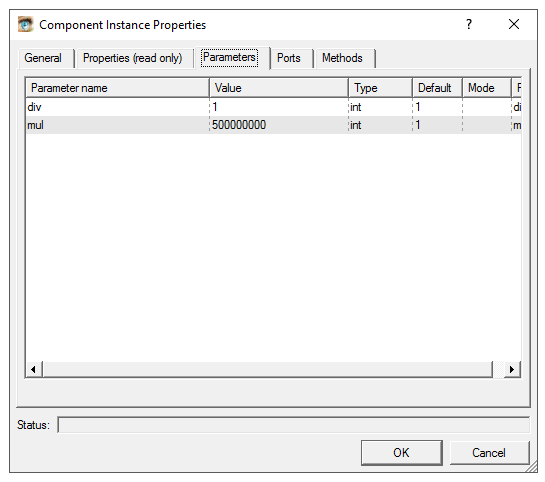
Stage 8: Configure FreeRTOSconfig.h
Well the screenshot below is self explanatory. Set the tick value to 100. Heap size to 1MB. The clock setting does not matter in this case or I don’t give a damn about it.


Stage 9: Build and Deploy
ARM-DS 5 will generally build everything provided you set it up properly. I assume that you know this. Setup the CPU type, apcs value, --unaligned-access for the C compiler, scatter loading file, entry point etc.

The final output will be a freertos.axf file in the debug directory (based on your settings) that needs to be converted to a bin file by using the fromelf utility.

fromelf --binary freertos.axf --output freertos.bin

The u-boot header mentioned earlier can be applied as

mkimage -A arm -O linux -T kernel -C none -a 0x80000000 -e 0x80000000 -n "Cortex A8 FreeRTOS" -d freertos.bin freertosimg

The freertosimg can now be copied to the sdcard.

To create the script file, first create a boot.cmd file with the contents
fatload mmc 0 80000000 freertosimg
bootm 80000000

Then execute mkimage as
mkimage –A arm –O linux –T kernel –C none –a 0 –e 0 –n “Cortex A8 Image” –d boot.cmd boot.scr

boot.scr can now be copied to the sdcard.

Insert the sdcard into the board and boot from mmc. If all goes well you should see your application running. In my case I just blinked the two user led’s on the board 
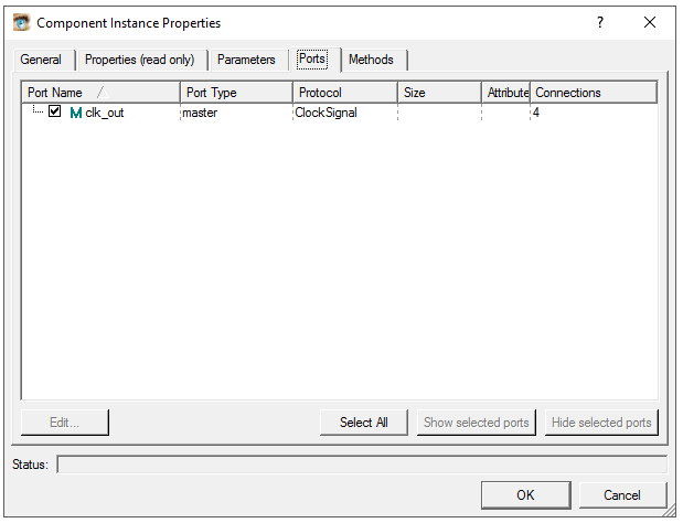
using the flash task that comes with the demo. Here are a few more screenshots of the process.

Debugging !!!

 Running !!!

Here is a Cinemagraph of the board and the LEDs
http://memories.nokia.com/en/images/aac17538-5d52-46fd-bdc1-03f200bbf2d3

A note – this was not meant to be a precise description but just a reference. You can use this to try deploying your FreeRTOS on any other board. This is a long write up & I could have missed something. If you get stuck trying this or have any questions please post them in the comments below. I will keep updating this post with newer items and “fixes”.

Thanks for watching.